LED (Light Emitting Diode) structure and manufacturing method thereof

A technology for light-emitting diodes and a manufacturing method, which is applied to electrical components, circuits, semiconductor devices, etc., can solve the problems of reducing the light-emitting efficiency of the light-emitting diode structure 124 and reducing the light-emitting area of ​​the light-emitting layer 108, so as to increase the overall light-emitting area and improve light extraction. rate, the effect of expanding the area

Inactive Publication Date: 2012-05-09
佛山市奇明光电有限公司 +1
View PDF4 Cites 17 Cited by
  • Summary
  • Abstract
  • Description
  • Claims
  • Application Information

AI Technical Summary

Problems solved by technology

However, if figure 1 As shown, increasing the area of ​​the n-type ohmic contact layer 116 and the n-type electrode 118 will relatively reduce the light-emitting area of ​​the light-emitting layer 108, which will reduce the light-emitting efficiency of the light-emitting diode structure 124

Method used


Image

  • LED (Light Emitting Diode) structure and manufacturing method thereof
  • LED (Light Emitting Diode) structure and manufacturing method thereof
  • LED (Light Emitting Diode) structure and manufacturing method thereof

Examples


Embodiment Construction

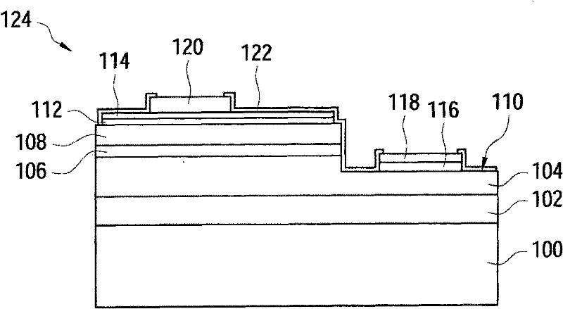
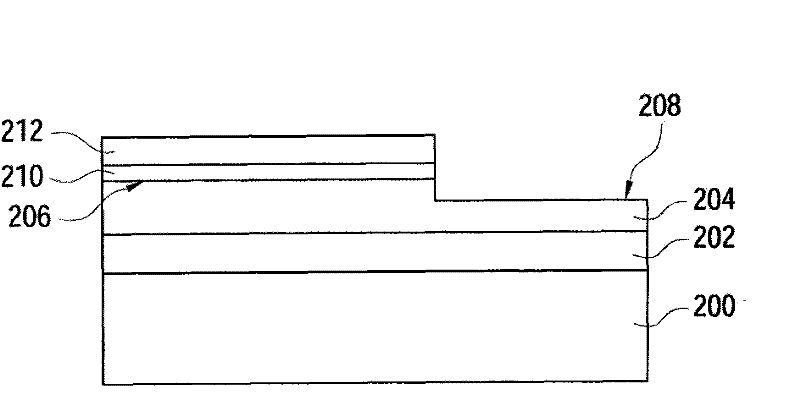
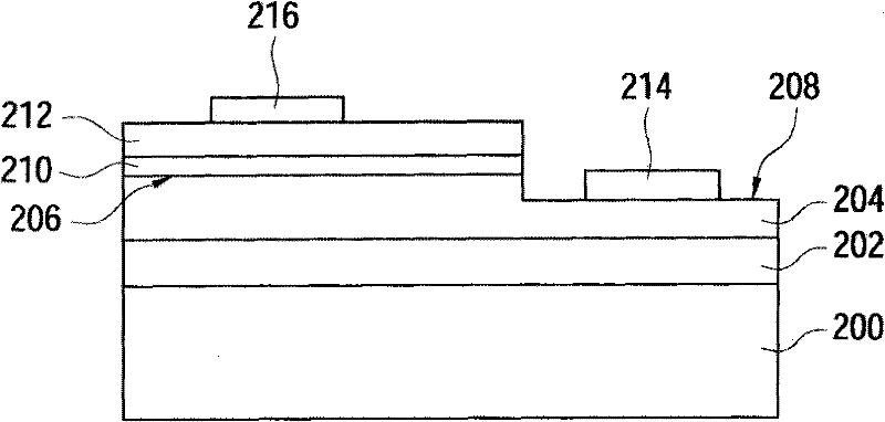
[0062] Please refer to Figure 2A to Figure 2E , which shows a process cross-sectional view of a light emitting diode structure according to an embodiment of the present invention. In this embodiment, first, a transparent substrate 200 is provided. The material of the substrate 200 can be, for example, sapphire. Next, the buffer layer 202 is selectively formed on the substrate 200 by epitaxy, such as metal organic chemical vapor deposition (MOCVD). The material of the buffer layer 202 can be an undoped semiconductor, such as undoped gallium nitride series materials. Next, a light-emitting epitaxial structure is grown on the buffer layer 202 by means of epitaxy, such as metalorganic chemical vapor deposition. In this embodiment, the light emitting epitaxial structure may include the first electrical type semiconductor layer 204 , the light emitting layer 210 and the second electrical type semiconductor layer 212 stacked on the buffer layer 202 in sequence. Wherein, the firs...


PUM


Abstract

The invention discloses an LED (Light Emitting Diode) structure and a manufacturing method thereof. The LED structure comprises a base plate, a light emitting epitaxy structure, a first electric contact layer, a second electric contact layer, a transparent insulating layer, a first reflection layer, a second reflection layer, a first barrier layer, a second barrier layer, a first electric electrode and a second electric electrode. The first electric contract layer and the second electric contact layer are respectively arranged on a first electric semiconductor layer and a second electric semiconductor layer which are in a light emitting epitaxy structure. The transparent insulating layer covers the light emitting epitaxy structure, the first electric contact layer and the second electric contact layer and comprises a first contact window and a second contact window which respectively expose the first electric contact layer and the second electric contact layer. The first reflection layer and the second reflection layer respectively cover the first contact window and the second contact window and extend on the transparent insulating layer. The first barrier layer and the second barrier layer respectively cover the first reflection layer and the second reflection layer. The first electric electrode and the second electric electrode are respectively arranged on the first barrier layer and the second barrier layer and fully fill the first contact window and the second contact window.

Description

technical field [0001] The present invention relates to a light-emitting structure, and in particular to a light-emitting diode (LED) structure and a manufacturing method thereof. Background technique [0002] Please refer to figure 1 , which shows a schematic cross-sectional view of a conventional LED structure. The LED structure 124 includes a substrate 100, a buffer layer 102, an n-type semiconductor layer 104, a light-emitting layer 106, a p-type semiconductor layer 108, a p-type ohmic contact layer 112, a reflective layer 114, an n-type ohmic contact layer 116, and an n-type electrode. 118 . The p-type electrode 120 and the passivation layer 122 . [0003] In the LED structure 124 , the buffer layer 102 is disposed on the substrate 100 . The n-type semiconductor layer 104 is provided on the buffer layer 102 . The light emitting layer 106 is disposed on a portion of the n-type semiconductor layer 104 such that the n-type semiconductor layer 104 has an exposed portion...

Claims


Application Information

Patent Timeline
Patent Type & Authority Applications(China)
IPC IPC(8): H01L33/00H01L33/36H01L33/38
Inventor 朱长信余国辉
Owner 佛山市奇明光电有限公司
Why Eureka
Try Eureka