


Quick Research
Generate reliable direction feasibility study reports for your R&D in just a few steps.

Technical Q&A
Discover and master advanced knowledge NOW. Basics, ideas, possibilities, all at once.

Find Solutions
As an expert in R&D theories, this can generate solutions to your technical problems instantly.

Evaluate Feasibility
Analyze your overall solution with one click, know your potential R&D risks in advance.

Monitor Landscape
Get weekly tech updates, stay abreast of the latest tech innovations and key insights.
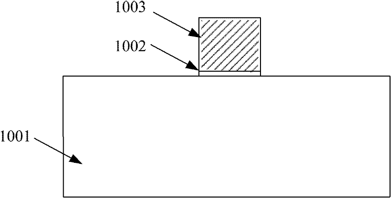
Formation method of salicide
A technology of metal silicide and silicon oxide, applied in the fields of electrical components, semiconductor/solid-state device manufacturing, semiconductor devices, etc. The difference in resistance value is relatively large, so as to achieve the effect of increasing the density and reducing the difference in resistance value per unit area
- Summary
- Abstract
- Description
- Claims
- Application Information
AI Technical Summary
Problems solved by technology
Method used
Image

Examples
Embodiment Construction
[0041] In order to make the object, technical solution and advantages of the present invention clearer, the solutions of the present invention will be further described in detail below with reference to the accompanying drawings and examples.
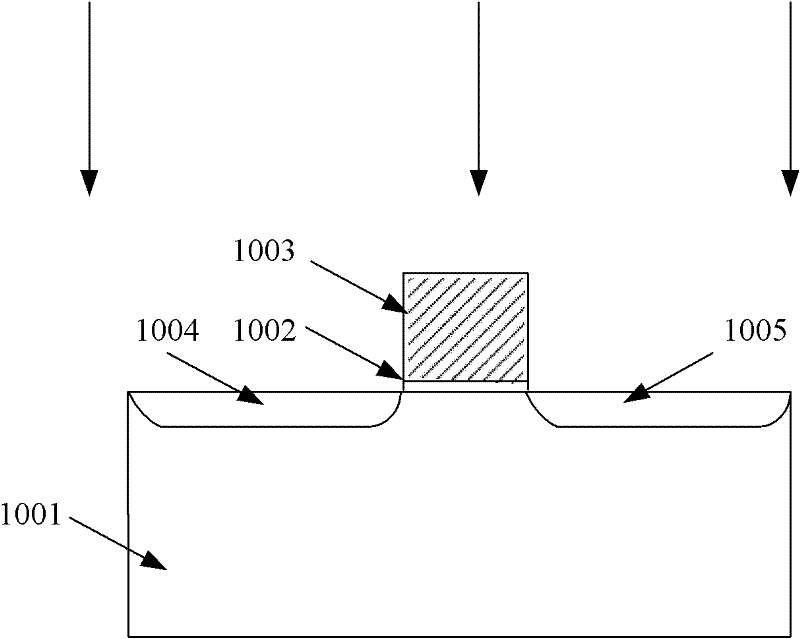
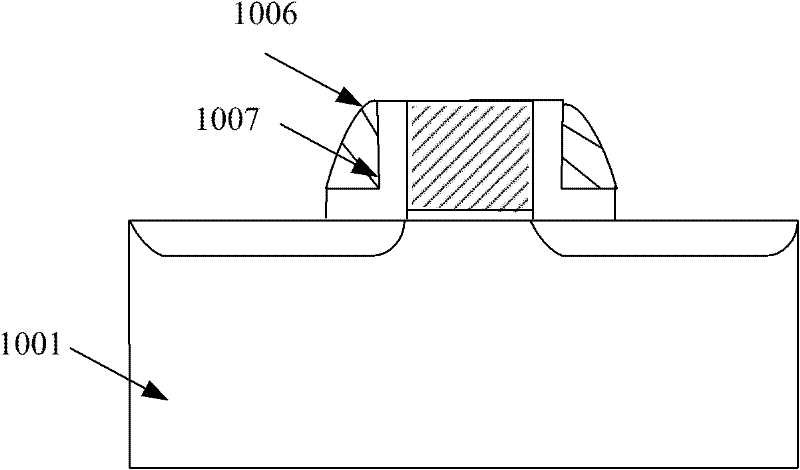
[0042]The core idea of the present invention is: after depositing the metal silicide barrier layer, thermal baking is performed, and then the metal silicide barrier layer is etched to expose the surface of the semiconductor substrate or the gate structure corresponding to the contact hole formation area. , deposit metal, and finally perform rapid annealing treatment to form metal silicide on the exposed semiconductor substrate surface or gate structure surface. Due to the thermal baking after depositing the metal silicide barrier layer, the metal silicide of the same batch of products The density of the barrier layer has been improved and stabilized at a substantially the same density. When subsequent rapid annealing is performed, the ...
PUM
 Abstract
Description
Claims
Application Information
 - R&D Engineer
- R&D Manager
- IP Professional
- Industry Leading Data Capabilities
- Powerful AI technology
- Patent DNA Extraction
Browse by: Latest US Patents, China's latest patents, Technical Efficacy Thesaurus, Application Domain, Technology Topic, Popular Technical Reports.
© 2024 PatSnap. All rights reserved.Legal|Privacy policy|Modern Slavery Act Transparency Statement|Sitemap|About US| Contact US: help@patsnap.com