PMOS radiation dosimeter based on silicon on insulator

A silicon-on-insulator, radiation dose technology, applied in dosimeters, semiconductor devices, electrical components, etc., achieves the effects of simple structure and manufacturing steps, improved integration, and reduced production costs and process difficulties

Inactive Publication Date: 2012-05-23
INST OF MICROELECTRONICS CHINESE ACAD OF SCI
View PDF2 Cites 13 Cited by
  • Summary
  • Abstract
  • Description
  • Claims
  • Application Information

AI Technical Summary

Problems solved by technology

This makes it possible to use the back gate of SOI devices for ionizing total dose radiation detection

Method used


Image

  • PMOS radiation dosimeter based on silicon on insulator
  • PMOS radiation dosimeter based on silicon on insulator
  • PMOS radiation dosimeter based on silicon on insulator

Examples


Embodiment Construction

[0024] The present invention will be described in further detail below in conjunction with the accompanying drawings.

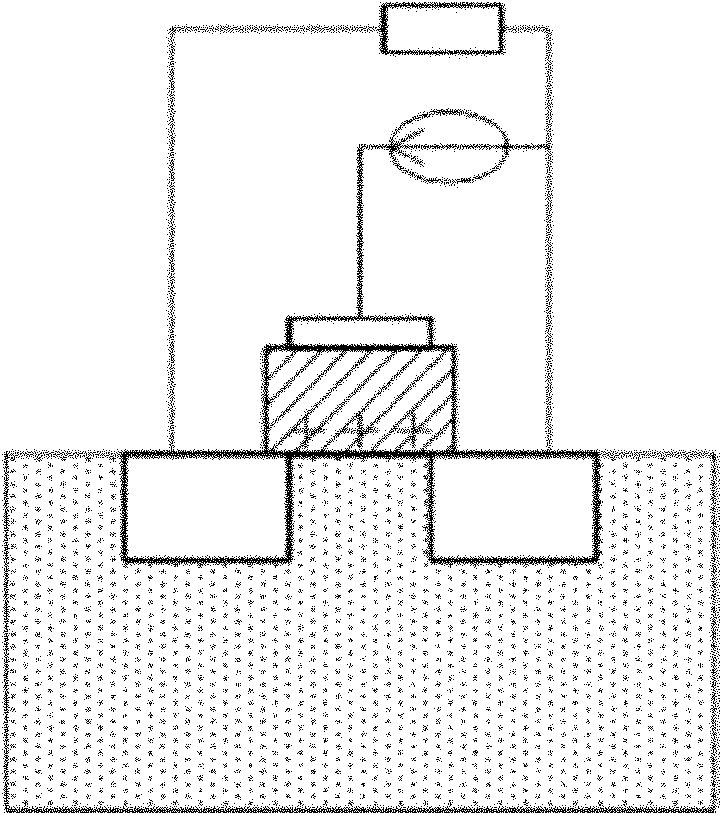
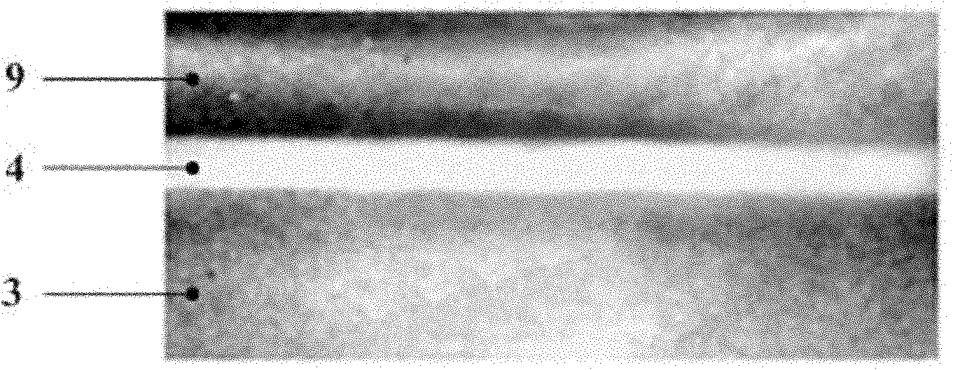
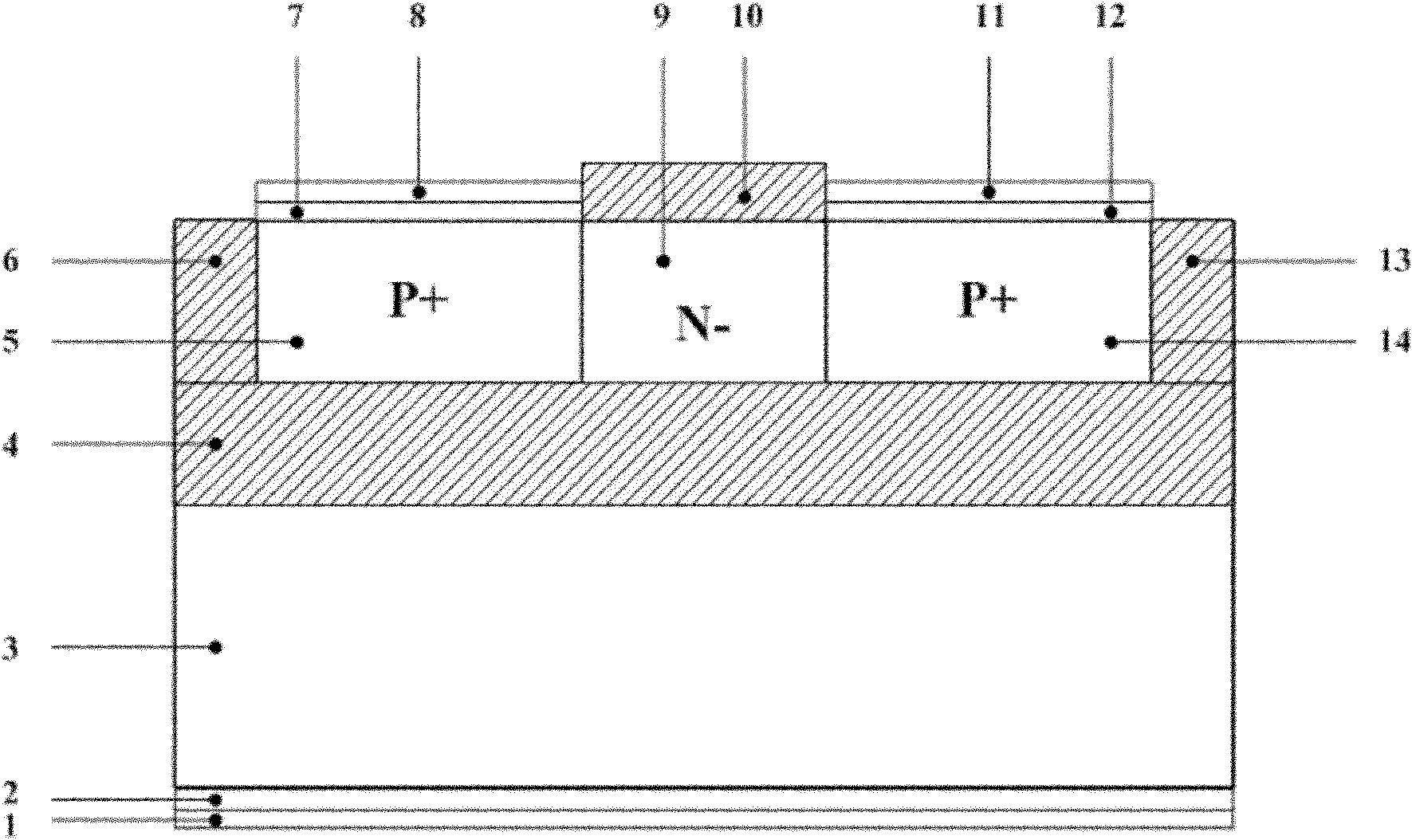
[0025] Such as image 3 as shown, image 3 It is a structural schematic diagram of a PMOS radiation dosimeter based on SOI technology provided by the present invention. The radiation dosimeter uses silicon-on-insulator (SOI) with the top silicon 9, the buried oxide layer 4 and the bottom silicon 3 from top to bottom as the basic structure. The radiation dosimeter includes:

[0026] A positive gate oxide layer 10 disposed on the upper surface of the top silicon layer 9;

[0027] The source region 5 disposed on the left side of the top silicon layer 9, the source region polycide layer 7 disposed on the upper surface of the source region 5, and the source electrode 8 disposed on the upper surface of the source region polycide layer 7;

[0028] a first isolation oxide region 6 disposed on the left side of the source region 5;

[0029] The drain region 14 disp...


PUM


Abstract

The invention relates to a PMOS radiation dosimeter based on a silicon on insulator. The PMOS radiation dosimeter comprises a silicon on insulator that successively includes top silicon, a buried oxide layer, and bottom silicon. Besides, the PMOS radiation dosimeter also comprises: a positive gate oxide layer, which is arranged on the upper surface of the top silicon; a source region, which is arranged at one side of the top silicon; a drain region, which is arranged at the other side of the top silicon; a source region polycrystalline silicide layer, which is arranged on the upper surface of the source region, and a source electrode, which is arranged on the upper surface of the source region polycrystalline silicide layer; a first isolation oxide region, which is arranged at one side of the source region; a drain region polycrystalline silicide layer, which is arranged on the upper surface of the drain region, and a drain electrode, which is arranged on the upper surface of the drain region polycrystalline silicide layer; a second isolation oxide layer, which is arranged at one side of the drain region; and a back gate metal layer, which is arranged on the lower surface of the bottom silicon, and a back gate electrode, which is arranged on the lower surface of the back gate metal layer. According to the invention, a PMOS radiation dosimeter with high sensitivity is provided; the manufacturing process of the dosimeter is compatible with an SOI CMOS technology; and an integrated level can be effectively improved.

Description

technical field [0001] The invention relates to the technical field of ionizing radiation dose measurement, in particular to a PMOS radiation dosimeter based on silicon-on-insulator. Background technique [0002] The space radiation environment is mainly a mixed field of high energy, continuum spectrum and various radiation components mainly charged high energy particles, and the incidence of particles is omnidirectional, and there are uncertainties and inhomogeneities in time and space. It brings some difficulties to radiation detection. The monitoring of the space radiation environment is mainly divided into active measurement methods and passive measurement methods. Active dose detectors mainly include ionization chambers, G-M counter tubes, proportional counter tubes and semiconductor detectors, while commonly used passive dosimeters for ionizing radiation mainly include pyrolysis Light detectors and nuclear track detectors. Although these technologies have achieved so...

Claims


Application Information

Patent Timeline
Patent Type & Authority Applications(China)
IPC IPC(8): G01T1/02H01L31/119H01L31/0352H01L31/0224
Inventor 刘梦新刘刚罗家俊韩郑生
Owner INST OF MICROELECTRONICS CHINESE ACAD OF SCI
Why Eureka
Try Eureka