Array substrate, liquid crystal display and manufacturing method of array substrate

An array substrate and manufacturing method technology, applied in the field of liquid crystal display, can solve the problems of lower product yield, etching Mura, and uneven developer concentration, etc., and achieve the effects of reducing manufacturing defect rate, reducing concentration difference, and eliminating influence

Active Publication Date: 2012-05-23
BOE TECH GRP CO LTD
View PDF3 Cites 17 Cited by
  • Summary
  • Abstract
  • Description
  • Claims
  • Application Information

AI Technical Summary

Problems solved by technology

[0007] However, in the prior art, when the gray-scale mask is used to prepare the first layer of transparent common electrodes, grid lines, and gate electrodes, the concentration of the developer in the adjacent pixel area will be different due to the formation of the driving circuit pattern on the peripheral driving circuit area. Uniform, resulting in the thickness of the photoresist exposed in the gray scale of the pixel area adjacent to the driving circuit pattern is significantly smaller than that of other pixel areas, which usually shows that there is a cloud-like Mura on the edge of the pixel area adjacent to the driving circuit pattern (such as Figure 2A shown)
This cloud-like Mura will affect the subsequent etching process, resulting in increased difficulty of the etching process and difficulty in controlling the parameters of the etching process, which in turn will cause the appearance of etching Mura, thereby reducing product yield.

Method used


Image

  • Array substrate, liquid crystal display and manufacturing method of array substrate
  • Array substrate, liquid crystal display and manufacturing method of array substrate
  • Array substrate, liquid crystal display and manufacturing method of array substrate

Examples


Embodiment 1

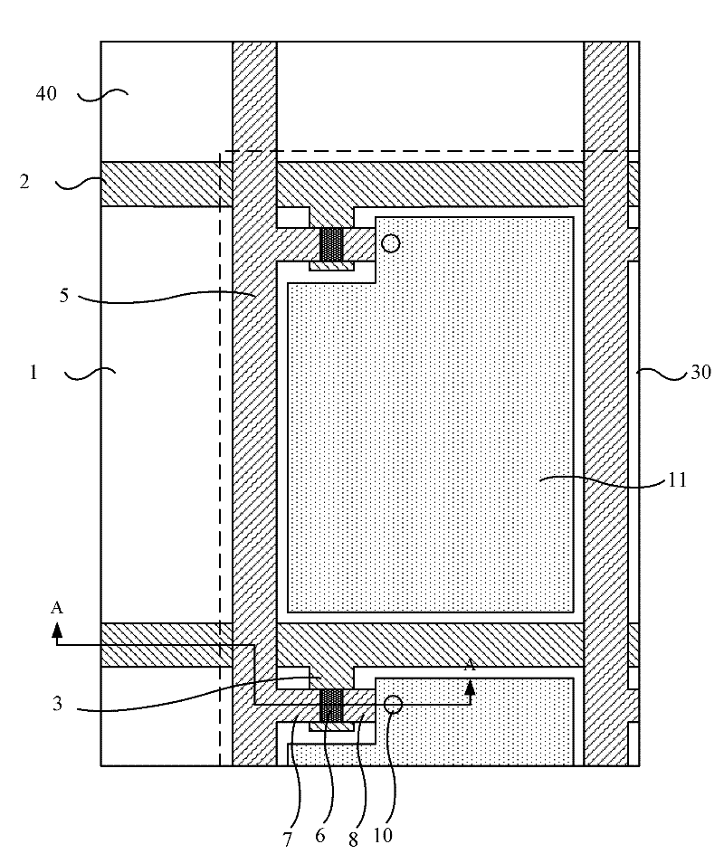
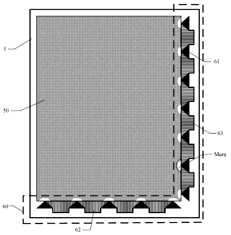
[0037] Figure 3A A schematic top view of the array substrate provided in Embodiment 1 of the present invention; Figure 3B for Figure 3A The enlarged schematic diagram of the common electrode driving interface pattern in the figure; Figure 3C for Figure 3A A schematic diagram of the positional relationship between the driver circuit area and the pixel area. Such as Figure 3A As shown, the array substrate of this embodiment includes: a base substrate 1 ; a pixel area 50 and a driving circuit area 60 are formed on the base substrate 1 .

[0038] Wherein, transparent common electrodes, data lines and gate lines intersecting horizontally and vertically are formed on the base substrate 1 located in the pixel area 50; the data lines and gate lines surround pixel units arranged in a matrix; each pixel unit includes a TFT Switch and pixel electrode; each TFT switch includes a gate electrode, a source electrode, a drain electrode and an active layer formed between the gate el...

Embodiment 2

[0048] Figure 4 It is a flow chart of the manufacturing method of the array substrate provided by Embodiment 2 of the present invention. Such as Figure 4 As shown, the manufacturing method of the present embodiment includes:

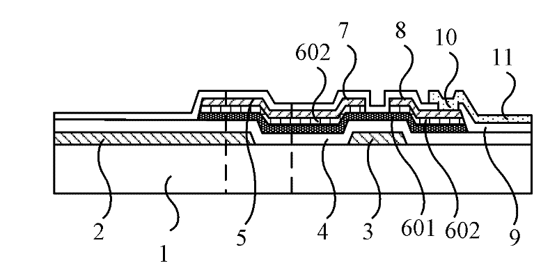
[0049] Step 401, sequentially depositing a transparent common electrode film and a gate metal film on the base substrate, and forming a pattern including a transparent common electrode, a gate line, a gate electrode, a common electrode drive interface pattern, and a gate line drive interface pattern through a patterning process; wherein, A slit is formed on the common electrode driving interface pattern, and each part of the common electrode driving interface pattern separated by the slit is connected to each other;

[0050] Step 402, sequentially deposit gate insulating layer film, active layer film and source-drain metal film on the base substrate formed with the above pattern, and form patterns including gate insulating layer, active layer, data l...

Embodiment 3

[0059] This embodiment provides a liquid crystal display, including components such as an outer frame, a liquid crystal panel, and a driving circuit. The liquid crystal panel is formed by combining the color filter substrate and the array substrate provided by the present invention, and a liquid crystal layer is filled therebetween. Wherein, the array substrate can adopt the array substrate provided by the embodiment of the present invention, and can be manufactured by using the manufacturing method of the array substrate provided by the embodiment of the present invention. The structure of the array substrate and the process flow of the method for manufacturing the array substrate will not be discussed in detail in this embodiment, and details can be referred to the above-mentioned embodiments of the present invention. Specifically, the outer frame is used to package the liquid crystal panel, and after the liquid crystal panel is packaged, it is connected with the driving cir...


PUM


Abstract

The invention discloses an array substrate, liquid crystal display and manufacturing method of array substrate; the array substrate comprises a substrate; the substrate comprises a pixel area and a driving circuit area; a common electrode driver interface pattern, a grid line driver interface pattern connected with the common electrode driver interface pattern and a data line driver interface pattern are formed on the substrate positioned in the driving circuit area; a slit is formed on the common electrode driver interface pattern; and various parts of the common electrode driver interface pattern separated by the slit are mutually connected. The technical scheme of the invention consumes the developer solution while the slit is formed on the common electrode driver interface pattern, reduces the influence of the periphery driving circuit area to the concentration of the developer solution in the adjacent pixel area, and improves the manufacturing yield of the array substrate.

Description

technical field [0001] The invention relates to liquid crystal display technology, in particular to an array substrate, a liquid crystal display and a manufacturing method of the array substrate. Background technique [0002] Liquid crystal display is a commonly used flat-panel display at present, among which thin film transistor liquid crystal display (ThinFilm Transistor Liquid Crystal Display; referred to as: TFT-LCD) has become the mainstream product in liquid crystal display due to its advantages of small size, low power consumption, and no radiation. . Usually TFT-LCD includes liquid crystal panel, drive circuit and backlight source. The liquid crystal panel is the main part of the TFT-LCD. It is composed of an array substrate and a color film substrate, and a liquid crystal layer is filled in between. By controlling the voltage provided by the drive circuit, the liquid crystal molecules are deflected in an orderly manner, resulting in light and dark changes of light....

Claims


Application Information

Patent Timeline
Patent Type & Authority Applications(China)
IPC IPC(8): G02F1/1362G02F1/1345H01L27/12H01L21/77
CPCG02F1/13458G02F2001/134372H01L27/124G02F1/1345G02F1/134372
Inventor 惠官宝
Owner BOE TECH GRP CO LTD
Why Eureka
Try Eureka