Semiconductor storage unit and device, and manufacturing method for semiconductor storage device

A storage unit and storage device technology, applied in the field of microelectronics, can solve problems such as poor data retention performance, and achieve the effects of improving data retention capabilities, improving storage characteristics, and high erasing speed

Inactive Publication Date: 2012-05-23
INST OF MICROELECTRONICS CHINESE ACAD OF SCI
View PDF9 Cites 11 Cited by
  • Summary
  • Abstract
  • Description
  • Claims
  • Application Information

AI Technical Summary

Problems solved by technology

[0004] In the process of realizing the present invention, the inventor realized that the prior art has the following defects: the storage unit using n-type doped polysilicon floating gate as the storage layer has a problem of data retention when the device feature size is getting smaller and smaller. Gradually worse performance

Method used


Image

  • Semiconductor storage unit and device, and manufacturing method for semiconductor storage device
  • Semiconductor storage unit and device, and manufacturing method for semiconductor storage device
  • Semiconductor storage unit and device, and manufacturing method for semiconductor storage device

Examples


Embodiment Construction

[0029] In order to make the object, technical solution and advantages of the present invention clearer, the present invention will be described in further detail below in conjunction with specific embodiments and with reference to the accompanying drawings.

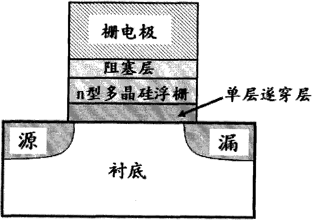
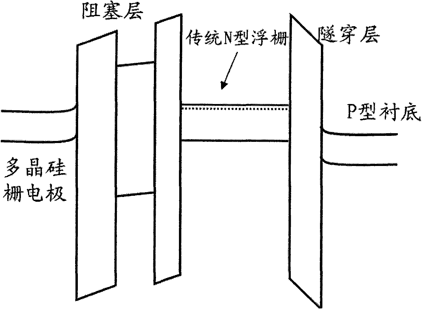
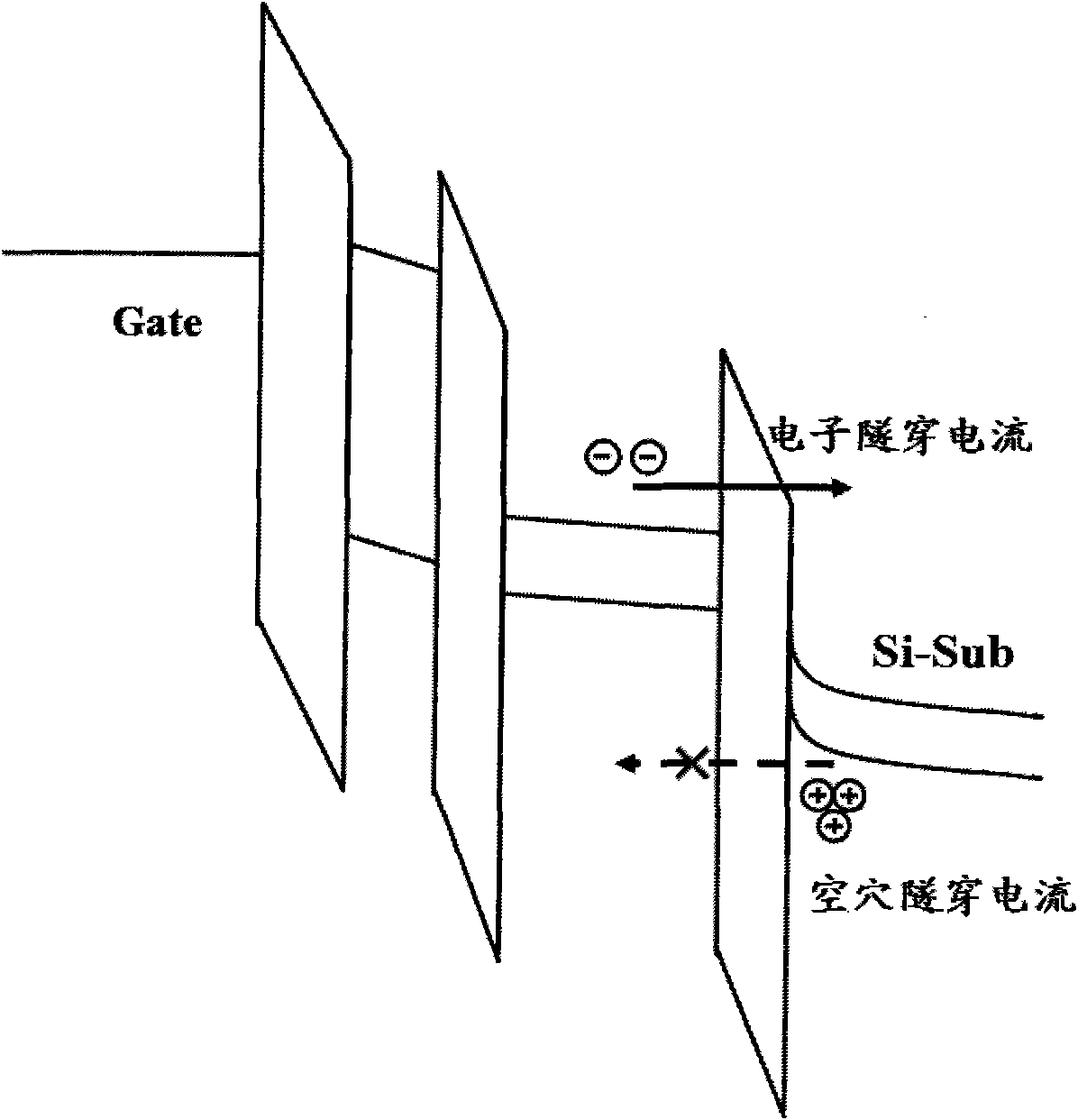
[0030] Aiming at the technical problem that the data retention performance of memory cells using n-type doped polysilicon floating gates as the storage layer in the prior art is getting smaller and smaller, the P-type doping can be used The polysilicon floating gate processed by means has a lower Fermi level than that of n-type doping, and electrons can be stored in a deeper potential well, which greatly improves the data retention performance. In addition, carbon doping treatment on the traditional polysilicon floating gate, or using SiC material (with the characteristics of wide band gap and deep conduction band) to replace the polysilicon film as the floating gate layer can also increase the electron storage potential w...


PUM


Abstract

The invention discloses a semiconductor storage unit and a semiconductor storage device, and a manufacturing method for the semiconductor storage device. In the semiconductor storage unit and the semiconductor storage device, P-type doping, carbon doping and other treatment processes are adopted by a polycrystalline silicon float gate of the conventional float gate device so as to obtain deeper electronic storage potential wells; therefore, data retention capacity of the device is improved. Tunneling layer barrier engineering that multiple layers of tunneling media are stacked is introduced, and a band structure of the device is adjusted so as to obtain high erasing speed; therefore, the comprehensive storage characteristic of the device is improved.

Description

technical field [0001] The invention relates to the technical field of microelectronics, in particular to a semiconductor storage unit, a device and a preparation method thereof. Background technique [0002] Floating gate structure memory is a mainstream memory type widely used and generally recognized at present. It is a very important semiconductor component and is widely used in the electronics and computer industries. Due to its own structure and material selection, the traditional floating gate memory has the limitations of requiring fast write / erase operations and long-term high-stability storage, and this contradiction has not been obvious as the technology node shrinks. Improvement limits the development of floating gate memory. Traditional floating gate memory cells use n-type doped polysilicon thin film floating gates for information storage. figure 1 It is a schematic diagram of a memory cell using an n-type doped polysilicon floating gate as a memory layer in ...

Claims


Application Information

Patent Timeline
Patent Type & Authority Applications(China)
IPC IPC(8): H01L29/788H01L29/49H01L27/115H01L21/336
Inventor 霍宗亮刘明金林刘璟张满红李冬梅
Owner INST OF MICROELECTRONICS CHINESE ACAD OF SCI
Why Eureka
Try Eureka