Low-resistance chip resistor and method of manufacturing same

A manufacturing method and low-resistance technology, applied in resistor manufacturing, resistors, thick-film resistors, etc., can solve the problems of increased self-heating of resistors, damage to protective film printed wiring boards, etc., to achieve high-precision manufacturing, enhanced electrical The effect of durability

Active Publication Date: 2012-05-23
KAMAYA ELECTRIC
View PDF6 Cites 0 Cited by
  • Summary
  • Abstract
  • Description
  • Claims
  • Application Information

AI Technical Summary

Problems solved by technology

Therefore, the self-heating of the resistor increases due to the requirement
In addition, there is a problem that the protective film of the resistor is damaged and the printed wiring board after mounting the resistor is damaged.

Method used


Image

  • Low-resistance chip resistor and method of manufacturing same
  • Low-resistance chip resistor and method of manufacturing same
  • Low-resistance chip resistor and method of manufacturing same

Examples


Embodiment 1

[0048] Hereinafter, the structure of the low-resistance chip resistor of this invention is demonstrated.

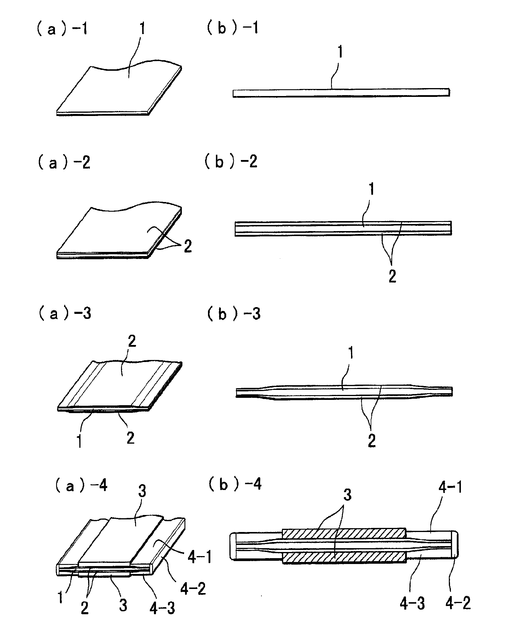
[0049] figure 1 (a) and (b) are a perspective view and a cross-sectional view of a long strip of an insulating substrate in which alumina powder, which is a type of ceramic powder, is dispersed in an epoxy resin at a volume ratio of 7:3. In these figures, metal plates made of iron-chromium-aluminum alloys, which are strip-shaped with a thickness of 0.05 mm and a width of 6.3 mm, and a length of about several meters, are laminated on several strip-shaped strips with a thickness of 0.3 mm and a width of 4.3 mm. The front and back sides of the substrate 1 of about m. A protective film 3 of epoxy resin with a thickness of about 10 μm is formed by screen printing in the long-dimension direction of the center of the upper and lower sides of the resistive film, and on the resistive layer 2 on both sides of the upper and lower protective film 3 1 and the end surface electrodes ...

Embodiment 1-1)

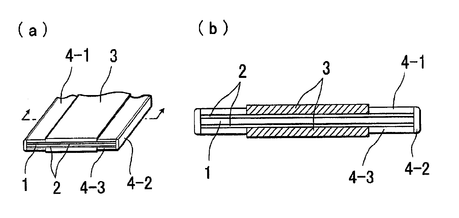
[0054] image 3 1 to 4 of (a) and (b) represent the above-mentioned Example 1 figure 1 A partial perspective view of the fabrication sequence of a low-resistance chip resistor and its cross-sectional view.

[0055] Figures (a)-1 and (b)-1 are insulating boards 1 in which alumina powder is dispersed and mixed in epoxy resin. The iron-chromium-aluminum alloy metal plate of the upper resistance layer is heated at 150°C to 200°C, and then press-rolled in the range of 2hPa to 3hPa, in (a)-3, (b)-3, and then up and down The above-mentioned epoxy resin is screen-printed in the central part, and baked at a temperature of 150°C to 250°C. In (a)-4 and (b)-4, the two ends are sequentially immersed in a chrome-nickel solution. Thereafter, baking is performed, and finally, as shown in (a)-4, cutting is carried out at intervals of, for example, 3.0 mm to 3.3 mm in width determined by a predetermined resistance value in a cross shape with respect to the longitudinal direction, and complete...

Embodiment 1-2)

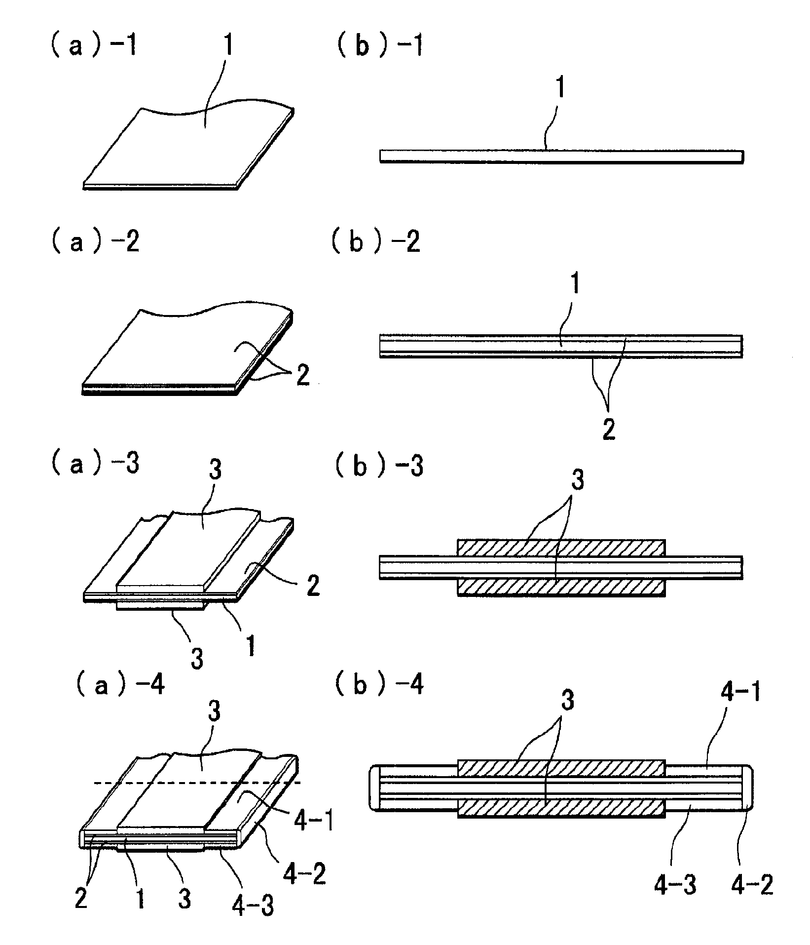
[0057] Figure 4 The illustrated embodiment is a modified example of the above (Embodiment 1-1).

[0058] The difference between this embodiment and (Example 1-1) is that when the resistive film 2 is hot-rolled on the insulating substrate 1, the two ends are made stronger than the central part in the width direction, that is, the central part is 1.5hPa Pressure rolling was performed while pressure rolling was performed at 3 hPa on both sides.


PUM

PropertyMeasurementUnit
Thicknessaaaaaaaaaa

Abstract

Provided are a low-resistance chip resistor having a simple structure in which self-independence is given and the mechanical strength is increased for durability, and an easier and faster method of manufacturing same. A low-resistance chip resistor characterized in that resistive layers are formed on both the front and back surfaces of an insulating substrate, or insulating substrates are formed on both the front and back surfaces of a resistive layer, that in the former, protective films are formed on the central portions of the resistive layers in the longitudinal direction and surface and back electrodes are formed on the resistive layers on both sides of the protective films, and in the latter, surface and back electrodes are formed on the resistive layers on both sides of the substrates, and that in both the former and latter, end surface electrodes are provided at both ends in the width direction.

Description

Technical field [0001] The invention involves a sheet resistor and its manufacturing method of sheet -shaped resistors, especially low resistors. Background technique [0002] Recently, in order to protect over currents such as portable portable devices that rushed into multi -functional portable devices, low -resistance value of the low -resistance value for current detection was used.Therefore, for the size, resistance value of the resistor, the same resistance, and being able to detect larger current values, the rated power is required to increase.Therefore, due to the requirements, the spontaneous heating of the resistor increased.In addition, the protective film of the resistor and the printed wiring board after the resistor is installed. [0003] Therefore, in patent literature 1, the mechanical strength of the component is used to enhance the mechanical strength of the component on the ceramic substrate 1. [0004] In addition, the following contents are made in patent doc...

Claims


Application Information

Patent Timeline
IPC IPC(8): H01C3/00
CPCH01C1/148H01C17/006H05K3/285H01C7/003H05K1/167H01C3/00H01C17/00
Inventor 松川修平野立树户田笃司
Owner KAMAYA ELECTRIC
Why Eureka
Try Eureka