Method for manufacturing transistor

A manufacturing method and transistor technology, applied in semiconductor/solid-state device manufacturing, semiconductor devices, electrical components, etc., can solve problems such as unstable device performance, improve quality, and avoid leakage current problems.

Active Publication Date: 2012-05-30
SEMICONDUCTOR MANUFACTURING INTERNATIONAL (BEIJING) CORP
View PDF6 Cites 8 Cited by
  • Summary
  • Abstract
  • Description
  • Claims
  • Application Information

AI Technical Summary

Problems solved by technology

[0011] In practice, it is found that the transistors made by the existing method have leakage current, and the performance of the device is unstable

Method used


Image

  • Method for manufacturing transistor
  • Method for manufacturing transistor
  • Method for manufacturing transistor

Examples


Embodiment Construction

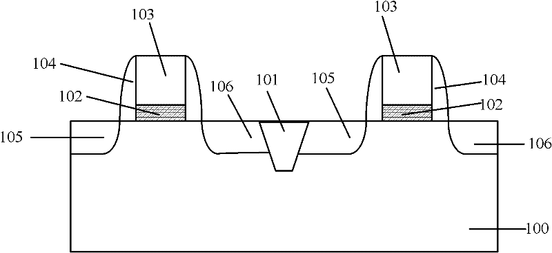
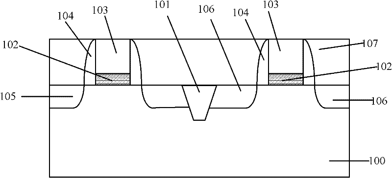
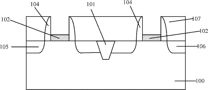
[0039] The transistors manufactured by the existing method using the high-K dielectric as the gate dielectric layer have leakage current, and the performance of the device is unstable. After research by the inventors, it is found that the leakage current of the transistor is caused by the damage of the gate dielectric layer by the etching process. Specifically, combined with image 3 , when performing an etching process to remove the dummy gate, using the dummy gate (made of polysilicon) and the interlayer dielectric layer (made of silicon oxide) 107 and the dummy gate and sidewalls (made of nitrogen) Silicon (Si) 104 has an etching selectivity, so there is no need to set a mask layer on the interlayer dielectric layer 107 and the sidewall 104, so that the surface of the interlayer dielectric layer 107 is exposed. However, the above etching process damages the gate dielectric layer 103 under the dummy gate, thus causing leakage current of the transistor.

[0040] The invento...


PUM


Abstract

The invention provides a method for manufacturing a transistor. The method comprises: a semiconductor substrate is provided; sacrificial layers are formed on the semiconductor substrate, wherein the sacrificial layers are formed by utilizing a deposition technology; dummy grids are formed on the sacrificial layers; source regions and drain regions are formed in portions of the semiconductor substrate, wherein the portions are at two sides of the dummy grids and the sacrificial layers; interlayer dielectric layers that are flush with the dummy grids are formed; wherein the interlayer dielectric layers covers the source regions and the drain regions; the dummy grids and the sacrificial layers are removed as well as grooves that are exposed outside the semiconductor substrate are formed in the interlayer dielectric layers; gate dielectric layers are formed at the bottom of the grooves; high K dielectric layers are formed at sidewalls and the bottoms of the grooves; and metal grids are formed on the high K dielectric layers, wherein the grooves are filled with the metal grids and are flush with the interlayer dielectric layers. According to the invention, a leakage current problem of a transistor can be solved as well as the performance of the transistor can be improved.

Description

technical field [0001] The invention relates to the technical field of semiconductors, in particular to a method for manufacturing transistors. Background technique [0002] As the feature size of integrated circuits shrinks to the deep submicron field, the gate size of transistors shrinks, and the thickness of the silicon dioxide layer as the gate dielectric layer also needs to be reduced accordingly to increase the gate capacitance of transistors and prevent devices from appearing. short channel effect. However, when the thickness of the gate dielectric layer is gradually reduced, and the thickness of the gate dielectric layer is reduced to less than 3 nanometers, many problems will arise, such as: (1) leakage current increases; (2) impurity diffusion, that is, the gate dielectric layer and the semiconductor substrate There is an impurity concentration gradient between them, and the impurity will diffuse from the gate into the semiconductor substrate or be fixed in the ga...

Claims


Application Information

Patent Timeline
Patent Type & Authority Applications(China)
IPC IPC(8): H01L21/336H01L21/28H01L21/316
Inventor 史运泽徐友锋刘焕新
Owner SEMICONDUCTOR MANUFACTURING INTERNATIONAL (BEIJING) CORP
Why Eureka
Try Eureka