Double-embedding structure and formation method thereof

A dual damascene structure and graphics technology, applied in the manufacture of electrical components, electrical solid devices, semiconductor/solid devices, etc., can solve problems such as difficult process control, affecting device performance, difficult electromigration and stress migration, etc., and achieves easy process Controlling, increasing feature size, reducing the effect of potential for electromigration and stress migration

Active Publication Date: 2014-03-12
SEMICON MFG INT (SHANGHAI) CORP +1
View PDF2 Cites 0 Cited by
  • Summary
  • Abstract
  • Description
  • Claims
  • Application Information

AI Technical Summary

Problems solved by technology

Figure 1d In the shown dual damascene structure, the height of the dielectric layer between the two through holes 14, that is, the etched dielectric layer 121 under the trench is relatively high, so the process in the method of forming the dual damascene structure is easy to control, However, because the height of the etched dielectric layer 121 below the trench is relatively high and the sidewall of the via hole 14 in contact with the dielectric layer 121 is vertical, this will cause the device to generate electromigration (electron migration, EM for short) and Stress migration (stress migration) problem, which affects the performance of the device
[0008] figure 2 It is a schematic cross-sectional view of another dual damascene structure formed by the method described above. In this dual damascene structure, the height of the dielectric layer 121 between the two through holes is relatively low and the through hole is in contact with the dielectric layer 121. Some parts have no vertical side walls, and the surface in contact with the filled metal is a circular arc surface, which is not easy to cause electromigration and stress migration problems, but the process is difficult to control

Method used


Image

  • Double-embedding structure and formation method thereof
  • Double-embedding structure and formation method thereof
  • Double-embedding structure and formation method thereof

Examples


Embodiment Construction

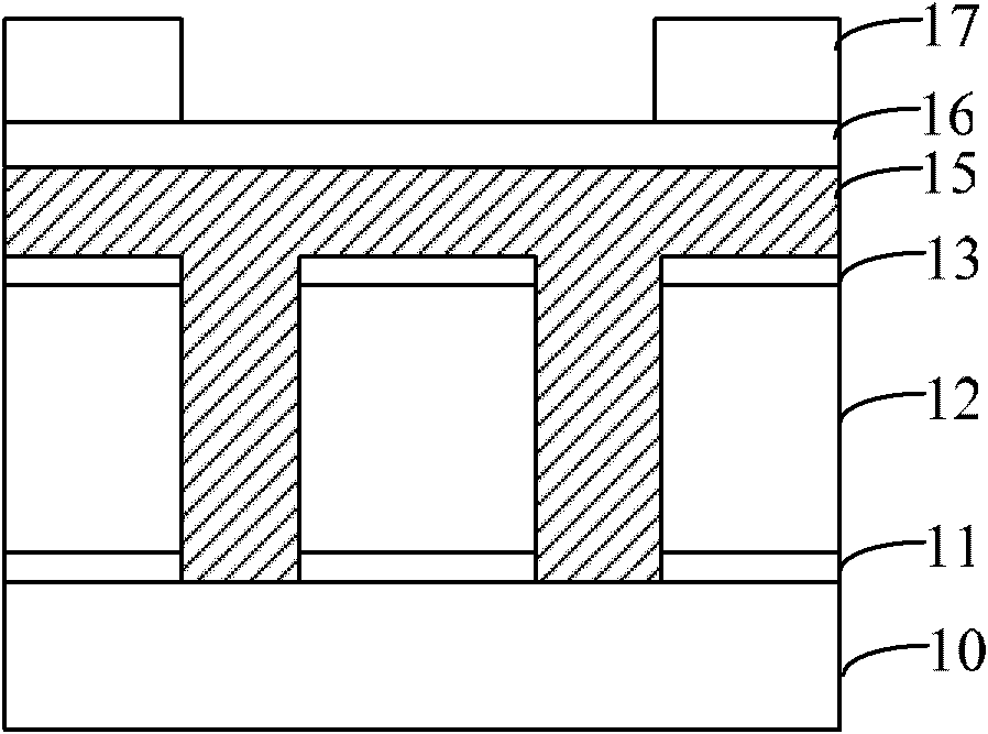
[0061] According to the method for forming a dual damascene structure according to a specific embodiment of the present invention, the etched dielectric layer below the formed trench (that is, the etched dielectric layer between the trench and the substrate) has a layer between the top surface and the bottom surface. The slope, due to the existence of the slope, can reduce the possibility of electromigration and stress migration; moreover, due to the existence of the slope, it is equivalent to increasing the characteristic size of the through hole, which can further reduce the generation of electromigration and stress migration possibility.

[0062] Moreover, in a specific embodiment, the method for forming a dual damascene structure uses the first step of etching and the second step of etching to form a trench, so that the etched dielectric layer under the trench has a layer between the top surface and the bottom surface. The height of the through hole is not reduced, that is...


PUM

PropertyMeasurementUnit
angleaaaaaaaaaa

Abstract

The invention provides a double-embedding structure and a formation method thereof. The method for forming the double-embedding structure comprises the following steps of: providing a substrate and sequentially forming a dielectric layer and a cap layer on the substrate; imaging the dielectric layer and the cap layer to form a first hole; forming an anti-reflecting layer, filling the first hole and covering the surface of the imaged cap layer; forming an imaged hard mask layer on the surface of the anti-reflecting layer and defining an image of a trench; taking the imaged hard mask layer as a mask and etching the anti-reflecting layer, the imaged cap layer and the imaged dielectric layer to form the trench and a through hole which are communicated with each other, wherein the through hole corresponds to the first hole, wherein the etched dielectric layer between the trench and the base is provided with a top surface, a bottom surface and an inclined surface; the bottom surface is located on the substrate, the top surface is opposite to the bottom surface and the inclined surface is located between the top surface and the bottom surface; removing the imaged hard mask layer and the residual anti-reflecting layer; and filling metal into the through hole and the trench. According to the invention, the possibility of generating electric migration and stress migration can be reduced.

Description

technical field [0001] The invention relates to the technical field of semiconductors, in particular to a double damascene structure and a forming method thereof. Background technique [0002] With the development of semiconductor technology, the integration level of integrated circuits is getting higher and higher, and the feature size (CD) of devices is getting smaller and smaller. Towards low-k (dielectric constant) materials. Subsequently, due to the use of low-k dielectric layers, the interconnection in integrated circuits has developed from aluminum interconnection technology to copper interconnection technology, and the commonly used copper interconnection structure is a dual damascene structure. As the CMOS process continues to develop towards smaller dimensions, when the device feature size develops to 65nm and below, the smaller feature size and larger aspect ratio will lead to poor copper filling ability, which will lead to serious electrical problems. Migration...

Claims


Application Information

Patent Timeline
Patent Type & Authority Patents(China)
IPC IPC(8): H01L21/768H01L23/522H01L23/528
Inventor 孙武张海洋周俊卿
Owner SEMICON MFG INT (SHANGHAI) CORP
Why Eureka
Try Eureka