Fabrication method of field-effect transistor and field-effect transistor

A technology of field effect transistors and manufacturing methods, applied in semiconductor/solid-state device manufacturing, electrical components, circuits, etc., to achieve the effects of good industrialization prospects, low cost, and simple process

Pending Publication Date: 2019-06-18
SHANGHAI IND U TECH RES INST
View PDF9 Cites 2 Cited by
  • Summary
  • Abstract
  • Description
  • Claims
  • Application Information

AI Technical Summary

Problems solved by technology

In the traditional field effect transistor, C S and C ins are all positive, resulting in (1+C S / C ins ) can never be less than 1, so it cannot be less than 60mV / dec. The negative capacitance effect of ferroelectric materials can make the ferroelectric capacitance negative, that is, C F <0

Method used


Image

  • Fabrication method of field-effect transistor and field-effect transistor
  • Fabrication method of field-effect transistor and field-effect transistor
  • Fabrication method of field-effect transistor and field-effect transistor

Examples


Embodiment Construction

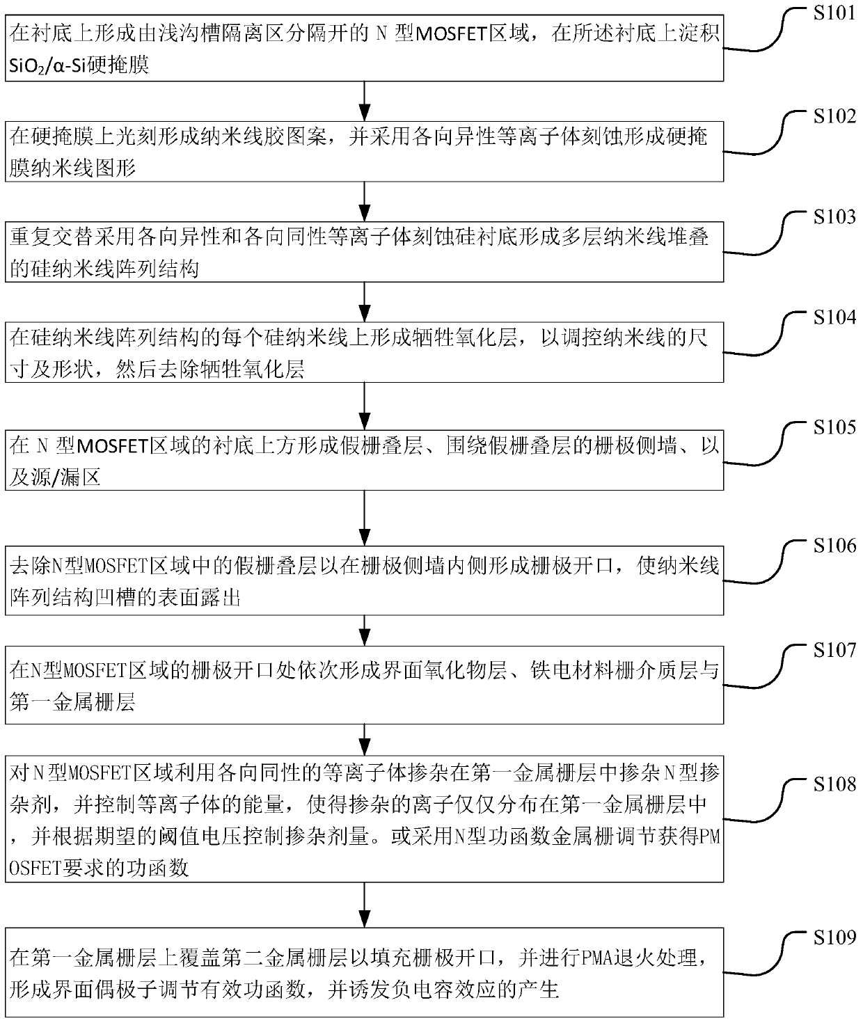
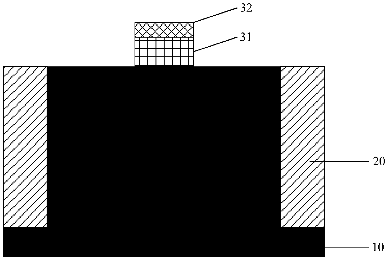
[0064] The present disclosure is to provide a ferroelectric material negative capacitance nanowire array ring gate NMOSFET structure and its manufacturing method, and fabricate a silicon nanowire array structure 40 in the N-type MOSFET region, wherein the silicon nanowire array structure 40 can be adopted by a silicon substrate 10 Anisotropic plasma etching and isotropic plasma etching are alternately etched, and at the same time, it is easier to realize the reduction of nanowire size by controlling the etching parameters, and obtain the desired nanowire size and cross-sectional shape; and through Nanowire sacrificial oxidation, using oxidation stress to further obtain the desired nanowire size and circular cross-sectional shape, to obtain the best gate control characteristics, while removing the surface damage of the nanowire, and retaining the electronic properties of the Si nanowire ring gate NMOSFET Good mobility. Moreover, because the nanowire ring-gate structure greatly ...


PUM

PropertyMeasurementUnit
thicknessaaaaaaaaaa
thicknessaaaaaaaaaa

Abstract

The invention discloses a fabrication method of a field-effect transistor and the field-effect transistor. The method comprises the steps of forming an N-type MOSFET region on a substrate, wherein theN-type MOSFET region is partitioned by a shallow groove isolation region; forming a hard mask pattern on the N-type MOSFET region; forming a silicon nanowire array structure, wherein the silicon nanowire array substrate comprises silicon nanowires which are stacked in a multi-layer way; forming a sacrifice oxide layer on the multi-layer stacked silicon nanowires to control the size and the morphology of the nanowires and remove the oxide layer; and sequentially forming an interface oxide layer, a ferroelectric material dielectric lamination layer and a metal gate lamination layer at the nanowire array structure. In the field-effect transistor, the gate control capability is greatly improved by a nanowire annular gate structure, and a short channel effect is prevented; and due to the introduction of a ferroelectric negative capacitance effect, the surface potential of the channel can be amplified, so that the nanowire NMOSFET has super steep sub-threshold slope and improved on / off current ratio.

Description

technical field [0001] The disclosure belongs to the technical field of semiconductors, and relates to a manufacturing method of a field effect tube and the field effect tube. Background technique [0002] As the feature size of integrated circuits becomes smaller and smaller, planar CMOS devices have encountered serious challenges, and various new device structures have emerged. The gate structure of devices has evolved from traditional planar single gates to double gates, triple gates, and completely wrapped channel. The gate-all-around structure, the gate-control ability and the ability to control the short channel effect are continuously enhanced, and the MOSFET with the nanowire gate-all-around structure (GAA) with quasi-ballistic transmission characteristics is widely used due to its strong gate control ability and the ability to reduce the size. Attach great importance to it and become a strong competitor in the technology generation of 3nm and below. However, when t...

Claims


Application Information

Patent Timeline
Patent Type & Authority Applications(China)
IPC IPC(8): H01L29/78H01L29/51H01L29/49H01L21/336
Inventor 徐秋霞胡正明陈凯
Owner SHANGHAI IND U TECH RES INST
Why Eureka
Try Eureka