

Preparation method of lead selenide semiconductor film
A lead selenide and semiconductor technology, which is applied in ion implantation plating, metal material coating process, coating, etc., can solve the problems that the film does not have photoconductive properties, poor stability, and complicated processing technology
- Summary
- Abstract
- Description
- Claims
- Application Information
AI Technical Summary
Problems solved by technology
Method used
Image

Examples
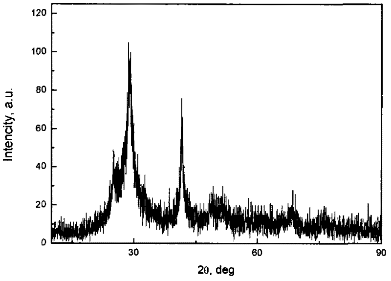
Embodiment 1
[0020] The glass substrate was ultrasonically cleaned in absolute ethanol and acetone for 10 minutes, then washed with deionized water, dried and placed in a vacuum chamber. The distance between the glass substrate and the target was 60 mm. Composite target with a purity of 99.99%, vacuumed to 3.9×10 -5 Pa. During the sputtering process, the working gas is high-purity argon, and the flow rate is 20cm 3 / min, the reaction gas is high-purity oxygen, and the gas flow rate is 2cm 3 / min, the working air pressure in the preparation process is 1.5×10 -1 Pa. The substrate is heated to 100°C. Bombard the surface of the substrate with a 50W power ion source in an argon atmosphere for 10 minutes to remove oxides and other impurities on the surface. Turn on the intermediate frequency power supply, the power is 100W, and feed oxygen at the same time, cut off the power supply after sputtering for 60 minutes, keep vacuum cooling, and take out the film for observation after cooling to r...
Embodiment 2
[0023] The glass substrate was ultrasonically cleaned in absolute ethanol and acetone for 10 minutes, then washed with deionized water, dried and placed in a vacuum chamber. The distance between the glass substrate and the target was 60 mm. Composite target with a purity of 99.99%, vacuumed to 3.6×10 -5 Pa. During the sputtering process, the working gas is high-purity argon, and the flow rate is 20cm 3 / min, the reaction gas is high-purity oxygen, and the gas flow rate is 1.5cm 3 / min, the working air pressure in the preparation process is 1.5×10 -1 Pa. The substrate is heated to 150°C. Bombard the surface of the substrate with a 50W power ion source in an argon atmosphere for 10 minutes to remove oxides and other impurities on the surface. Turn on the intermediate frequency power supply, the power is 150W, and feed oxygen at the same time, cut off the power supply after sputtering for 90 minutes, keep vacuum cooling, and take out the film for observation after cooling to...
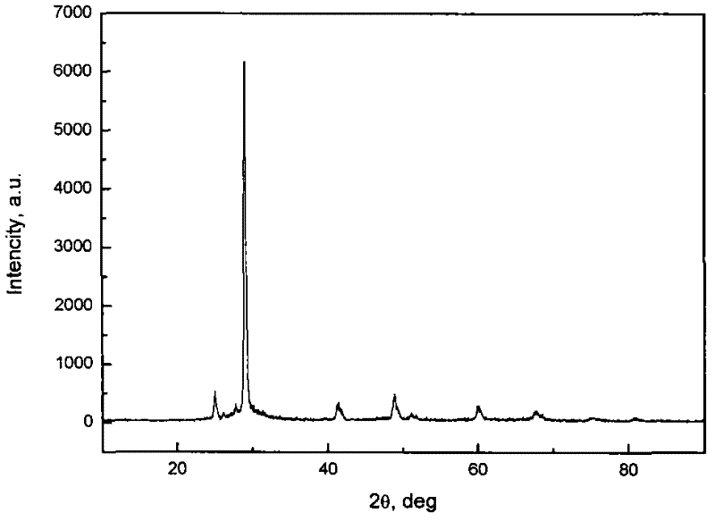
Embodiment 3
[0026] The glass substrate was ultrasonically cleaned in absolute ethanol and acetone for 10 minutes, then washed with deionized water, dried and placed in a vacuum chamber. The distance between the glass substrate and the target was 60 mm. Composite target with a purity of 99.99%, vacuumed to 3.9×10 -5 Pa. During the sputtering process, the working gas is high-purity argon, and the flow rate is 20cm 3 / min, no reaction gas is introduced in this embodiment, which is used for photoelectric performance comparison test. The working air pressure in the preparation process is 1.5×10 -1 Pa. The substrate is heated to 100°C. Bombard the surface of the substrate with a 50W power ion source in an argon atmosphere for 10 minutes to remove oxides and other impurities on the surface. Connect the intermediate frequency power supply, the power is 100W. Cut off the power supply after sputtering for 60 minutes, keep vacuum cooling, and take out the film for observation after cooling to ...
PUM
 Abstract
Description
Claims
Application Information