Device for thinning multi-layer material and method for thinning to-be-detected sample

A multi-layer material and sample technology, applied in measurement devices, instruments, scanning probe microscopy, etc., can solve the problems of inability to accurately measure the etching depth, inability to accurately locate, and solve the problem of in-situ etching control Effect

Inactive Publication Date: 2012-06-27
SUZHOU INST OF NANO TECH & NANO BIONICS CHINESE ACEDEMY OF SCI
View PDF7 Cites 7 Cited by
  • Summary
  • Abstract
  • Description
  • Claims
  • Application Information

AI Technical Summary

Problems solved by technology

The disadvantage of using scanning electron microscopy and other methods to observe is that because the secondary electron imaging measurement is a two-dimen...

Method used


Image

  • Device for thinning multi-layer material and method for thinning to-be-detected sample
  • Device for thinning multi-layer material and method for thinning to-be-detected sample
  • Device for thinning multi-layer material and method for thinning to-be-detected sample

Examples


Embodiment 1

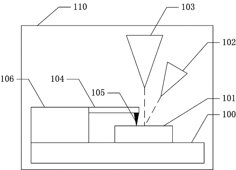
[0032] figure 1 Shown is a thinning device for a multi-layer material provided by the present invention, including a reaction chamber 110, an atomic force microscope, a focused ion beam device 103, an electron microscope 102 and a sample stage 100, and the sample stage 100, The focused ion beam device 103, the atomic force microscope and the electron microscope 102 are located in the reaction chamber 110; the sample stage 100 is used to place the sample to be tested; the atomic force microscope is used to measure the surface contact potential difference of the sample to be tested, including a conductive probe 105 and a microcantilever 104 and the control device 106; the focused ion beam device 103 is used to etch the sample to be tested; the conductive probe 105 is used to contact the sample to be tested and measure the contact potential difference between the conductive probe and the sample to be tested; the microcantilever 104, It is used to move the conductive probe 105; th...

Embodiment 2

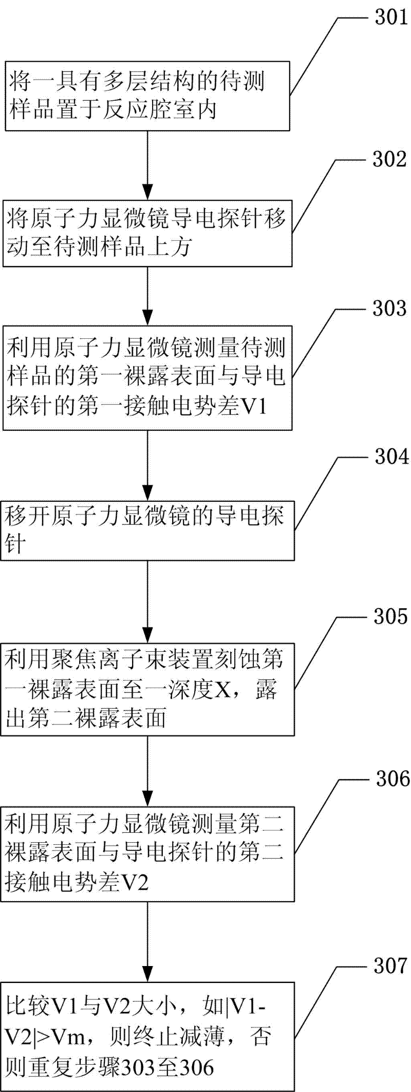
[0034] figure 2 Shown is the flow chart of the second step of the method embodiment of thinning the sample to be tested provided by the present invention, including: step 301, placing a sample to be tested with a multilayer structure in the reaction chamber; step 302, placing the conductive probe of the atomic force microscope The needle is moved above the sample to be tested; step 303, using the atomic force microscope to measure the first contact potential difference V1 between the first exposed surface of the sample to be tested and the conductive probe; step 304, removing the conductive probe of the atomic force microscope; step 305, using The focused ion beam device etches the first exposed surface to a depth X to expose the second exposed surface; step 306, uses an atomic force microscope to measure the second contact potential difference V2 between the second exposed surface and the conductive probe; step 307, compares V1 and V2 If the size is |V1-V2|>Vm, then the thin...

Embodiment 3

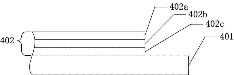
[0053] Figure 5 Shown is a schematic diagram of the structure of the sample to be tested in Embodiment 3 of the method for thinning the sample to be tested provided by the present invention. The sample to be tested 206 has a multilayer heterojunction structure, including p + GaAs layer 205, p + AlGaAs layer 204, p + GaAs layer 203, InGaAs layer 202, n - GaAs layer 201, n + GaAs layer 200 and n - GaAs substrate layer 210 . In addition, the layer thicknesses of the above-mentioned layer structures are 0.5 μm, 0.03 μm, 0.5 μm, 0.02 μm, 2 μm, and 0.5 μm, respectively.

[0054] The method for thinning the sample to be tested 206 includes: placing the sample to be tested 206 in a reaction chamber; imaging the designated etching region and the position of the conductive probe of the p+GaAs layer 205 of the sample through an electron microscope, and at the same time moving the microcantilever Conductive probe, under the guidance of the electron microscope image, move the condu...


PUM

PropertyMeasurementUnit
Layer thicknessaaaaaaaaaa

Abstract

The invention provides a device for thinning a multi-layer material and a method for thinning a to-be-detected sample, belonging to the field of testing of semiconductors. The device comprises a reaction chamber, an atomic force microscope, an electron microscope and a sample table. The sample table, the atomic force microscope and the electron microscope are positioned in the reaction chamber. The method for thinning the to-be-detected sample comprises the following steps of: putting a sample in the reaction chamber; measuring first contact potential difference V1 of a first bared surface of the to-be-detected sample; moving away a conducting probe of the atomic force microscope; etching the first bared surface at the depth X to expose a second surface; measuring first contact potential difference V2 of a second bared surface of the to-be-detected sample; and comparing the V1 with the V2 to judge whether to etch continuously. The device and the method disclosed by the invention are used for solving the problem of being incapable of precisely dissecting in the prior art. The device and the method are capable of precisely dissecting hetero-junction devices and have important meanings on preparation and property research of semiconductor devices.

Description

technical field [0001] The invention relates to the field of semiconductor device testing, in particular to the precise anatomy of a heterojunction device. Background technique [0002] For semiconductor heterojunction devices such as high-efficiency multi-junction solar cells and LEDs, the device structure often includes several or even dozens of heterojunction layers, and device functions such as photoelectric conversion are realized through these heterojunction interfaces. The properties of each layer, including layer thickness, composition and doping concentration, are different and affect the overall performance of the device. In order to test and analyze the properties of each layer, it is usually necessary to dissect the grown device, expose the surface of the layer to be measured, measure its parameters layer by layer, or make cross-sectional slices, and use transmission electron microscopy and other methods for observation. [0003] One method of accurately dissect...

Claims


Application Information

Patent Timeline
IPC IPC(8): G01Q30/20G01Q60/02
Inventor 刘争晖徐耿钊钟海舰樊英民曾雄辉王建峰周桃飞邱永鑫徐科
Owner SUZHOU INST OF NANO TECH & NANO BIONICS CHINESE ACEDEMY OF SCI
Why Eureka
Try Eureka