
Production method of semiconductor discrete device back side metal suitable for screen printing

A backside metal, discrete device technology, applied in semiconductor devices, semiconductor/solid-state device manufacturing, metal material coating processes, etc., can solve problems such as Ti/Ni/Ag structure falling off

Active Publication Date: 2012-06-27
HANGZHOU LION MICROELECTRONICS CO LTD
View PDF10 Cites 12 Cited by
  • Summary
  • Abstract
  • Description
  • Claims
  • Application Information

AI Technical Summary

Problems solved by technology

However, in the chip packaging process, some manufacturers will use a process called screen printing, that is, a solder layer is formed on the die on the front of the chip by means similar to printing. Due to the action of high temperature and nitrogen, it is easy to cause the Ti / Ni / Ag structure to fall off

Method used


Image

  • Production method of semiconductor discrete device back side metal suitable for screen printing
  • Production method of semiconductor discrete device back side metal suitable for screen printing

Examples


Embodiment Construction

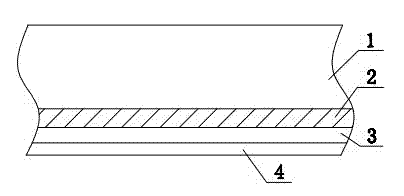
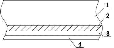
[0028] By evaporating metal on the back of the wafer 1 by the method of the present invention, a multilayer metal structure consisting of wafer 1, Cr2, Ni3 and Ag4 from top to bottom is finally obtained.

[0029] Processing step of the present invention is as follows:

[0030] 1) Film attachment: the wafer with the front structure of the device has been completed, and the UV film is pasted on the front of the wafer to protect the front structure of the wafer from damage during subsequent processing;

[0031] 2) Thinning the wafer by mechanical grinding: first rough grinding, using a 320-mesh grinding wheel to grind off the silicon on the back of the 300um wafer, and then finely grinding, using a 2000-mesh grinding wheel to grind off the silicon on the back of the 30um wafer. The model of the mechanical grinding machine: DFG8540, the manufacturer : DISCO;

[0032] 3) Relieve stress corrosion, remove the mechanical damage caused by step 2, the cleaning steps are as follows:

...


PUM


Abstract

The invention belongs to the semiconductor device manufacture field, concretely relating to a production method of semiconductor discrete device back side metal suitable for screen printing. Processing steps of the invention comprises: (1) pasting a film; (2) thinning a wafer through mechanical grinding; (3) removing stress corrosion; (4) carrying out wafer surface treatment before metal deposition; (5) removing a UV film pasted in step (1); (6) carrying out wafer back side metal evaporation. According to the invention, multilayer metal of a Cr / Ni / Ag structure is grown at a back side of the wafer, the multilayer metal and production technology of the above multilayer metal are different from a multilayer metal structure of a Ti / Ni / Ag structure and production technology of the multilayer metal structure of the Ti / Ni / Ag structure, since Cr is easy to form alloy with silicon at high temperature, under the premise that the metal and the silicon form ohmic contact, that the metal and the silicon do not drop off in welding is ensured, and a requirement of screen printing technology is met. According to the invention, the metal Ni can be substituted by metal NiV, and Ag can be substituted by Au.

Description

technical field [0001] The invention belongs to the field of semiconductor device manufacturing, in particular to a method for producing back metal of semiconductor discrete devices suitable for screen printing. Background technique [0002] The backside metallization process is a very important process for the production of discrete devices. For current high-current power devices, the mainstream backside metallization process in China is Ti / Ni / Ag three-layer metal structure, and the substrate is heavily doped material Sheet, this structure can make good ohmic contact between metal and silicon, and make the metal adhere to silicon better at the same time. However, in the chip packaging process, some manufacturers will use a process called screen printing, that is, a layer of solder layer is formed on the die on the front of the chip by means similar to printing. Due to the action of high temperature and nitrogen, it is easy to cause the falling off of the Ti / Ni / Ag structure...

Claims


Application Information

Patent Timeline
IPC IPC(8): H01L21/28H01L21/285C23C14/16C23C14/30
Inventor 朱春生周诗雨王艳萍汤林斌张瑞丽黄力平徐林海
Owner HANGZHOU LION MICROELECTRONICS CO LTD
Learn More