Reversal laminated organic light emitting diode
A technology of light-emitting diodes and organic light-emitting layers, which is applied in the directions of light-emitting materials, electrical components, and electrical solid-state devices, and can solve the problems of poor stability, high driving voltage, and low efficiency.
- Summary
- Abstract
- Description
- Claims
- Application Information
AI Technical Summary
Problems solved by technology
Method used
Image
Examples
Embodiment 1
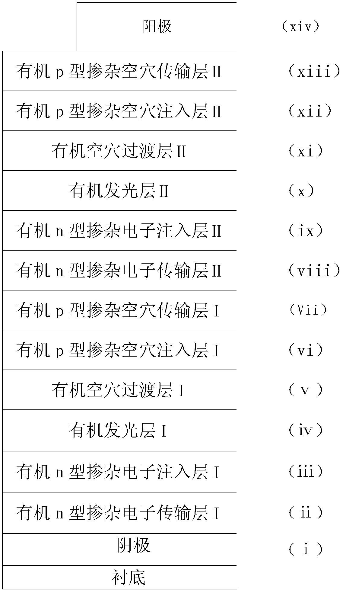
[0060] The structure is ITO / NTCDA:Pyronin B=1:0.5, thickness 5nm / Bphen:Rb 2 CO 3 =1:0.5, thickness 5nm / Alq3 thickness 40nm / mCP thickness 40nm / CBP:ReO 3 =1:0.5, thickness 5nm / 2-TNATA:ReO 3 =1:0.5, thickness 5nm / NTCDA:Pyronin B=1:0.5, thickness 5nm / Bphen:Rb 2 CO 3 =1:0.5, thickness 5nm / Alq3 thickness 40nm / mCP thickness 40nm / CBP:ReO 3 =1:0.5, thickness 5nm / 2-TNATA:ReO 3 =1:0.5, an inverted stack organic light-emitting diode with a connection layer structure consisting of double p-type doped layers and double n-type doped layers with a thickness of 5nm / Ag and a thickness of 100nm.
[0061] The organic light-emitting diode is composed of an ITO cathode, a layer of NTCDA deposited on the ITO cathode with a thickness of 5nm: Pyronin B=1:0.5 organic n-type doped electron transport layer I, a layer deposited on NTCDA: Pyronin B organic n-type Doping the electron transport layer I with Bphen:Rb with a thickness of 5 nm 2 CO 3 =1:0.5 Organic n-type doped electron injection layer ...
Embodiment 2
[0103] The structure is a layer of translucent gold covered on the glass substrate, the thickness is 20nm / NTCDA:Pyronin B=1:0.01, the thickness is 1000nm / Bphen:Rb 2 CO 3 =1:0.01, thickness 10nm / Alq3 thickness 60nm / mCP thickness 60nm / CBP:ReO 3 =1:0.01, thickness 10nm / 2-TNATA:ReO 3 =1:0.01, thickness 10nm / NTCDA:Pyronin B=1:0.01, thickness 10nm / Bphen:Rb 2 CO 3 =1:0.01, thickness 10nm / Alq3 thickness 60nm / mCP thickness 60nm / CBP:ReO 3 =1:0.01, thickness 10nm / 2-TNATA:ReO 3 =1:0.01, a reverse stack organic light-emitting diode with a connection layer structure consisting of double p-type doped layers and double n-type doped layers with a thickness of 1000nm / Ag with a thickness of 100nm.
[0104] The organic light-emitting diode is composed of a layer of translucent gold cathode with a thickness of 20nm covered on a glass substrate, and a layer of NTCDA:Pyronin B=1:0.01 organic n-type doped with a thickness of 1000nm deposited on the gold cathode. Electron transport layer I, a la...
Embodiment 3
[0136] The structure is a layer of translucent silver covered on the glass substrate, the thickness is 20nm / NTCDA:Pyronin B=1:0.2, the thickness is 500nm / Bphen:Rb 2 CO 3 =1:0.2, thickness 1nm / Alq3 thickness 50nm / mCP thickness 50nm / CBP:ReO 3 =1:0.2, thickness 1nm / 2-TNATA:ReO 3 =1:0.2, thickness 1nm / NTCDA:Pyronin B=1:0.2, thickness 1nm / Bphen:Rb 2 CO 3 =1:0.2, thickness 1nm / Alq3 thickness 50nm / mCP thickness 50nm / CBP:ReO 3 =1:0.2, thickness 1nm / 2-TNATA:ReO 3 =1:0.2, an inverted stack organic light-emitting diode with a connection layer structure consisting of double p-type doped layers and double n-type doped layers with a thickness of 5nm / Ag with a thickness of 100nm.
[0137] The organic light-emitting diode is composed of a layer of translucent silver cathode with a thickness of 20nm covered on a glass substrate, and a layer of NTCDA:Pyronin B=1:0.2 organic n-type doped electrons with a thickness of 500nm deposited on the silver cathode. Transport layer I, a layer of Bphe...
PUM
| Property | Measurement | Unit |
|---|---|---|
| Thickness | aaaaa | aaaaa |
| Thickness | aaaaa | aaaaa |
| Thickness | aaaaa | aaaaa |
Abstract
Description
Claims
Application Information


