Eureka AIR delivers breakthrough ideas for toughest innovation challenges, trusted by R&D personnel around the world.

Clock generation circuit used in analog-to-digital converter (ADC) with high speed and high precision

A clock generation circuit, analog-to-digital converter technology, applied in the direction of analog conversion, code conversion, electrical components, etc., can solve the problems of interference signal sampling, precision reduction, etc., to achieve the effect of improving precision and avoiding increased requirements

Inactive Publication Date: 2015-01-14
TSINGHUA UNIV
View PDF3 Cites 0 Cited by
  • Summary
  • Abstract
  • Description
  • Claims
  • Application Information

AI Technical Summary

Problems solved by technology

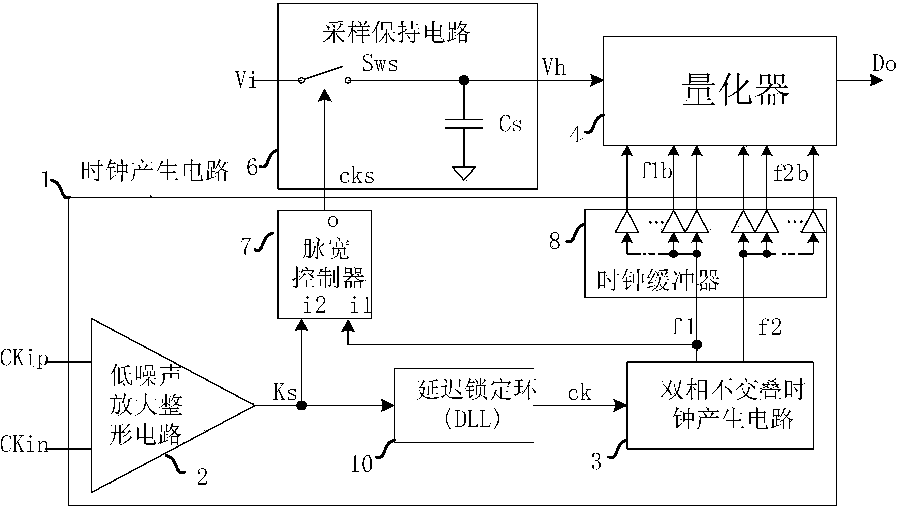
[0008] 2) The switching sampling action controlled by the falling edge of clock cks is ahead of the falling edge of f1b, which may interfere with the signal sampling controlled by the falling edge of f1b in quantizer 4, resulting in a decrease in its accuracy

Method used


Image

  • Clock generation circuit used in analog-to-digital converter (ADC) with high speed and high precision
  • Clock generation circuit used in analog-to-digital converter (ADC) with high speed and high precision
  • Clock generation circuit used in analog-to-digital converter (ADC) with high speed and high precision

Examples


Embodiment Construction

[0044] In order to make the object, technical solution and advantages of the present invention clearer, the present invention will be described in detail below in conjunction with the accompanying drawings and specific embodiments.

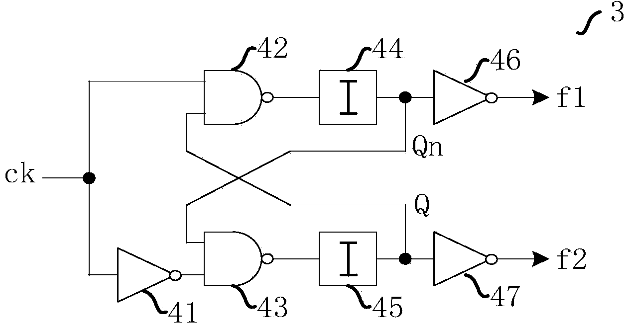
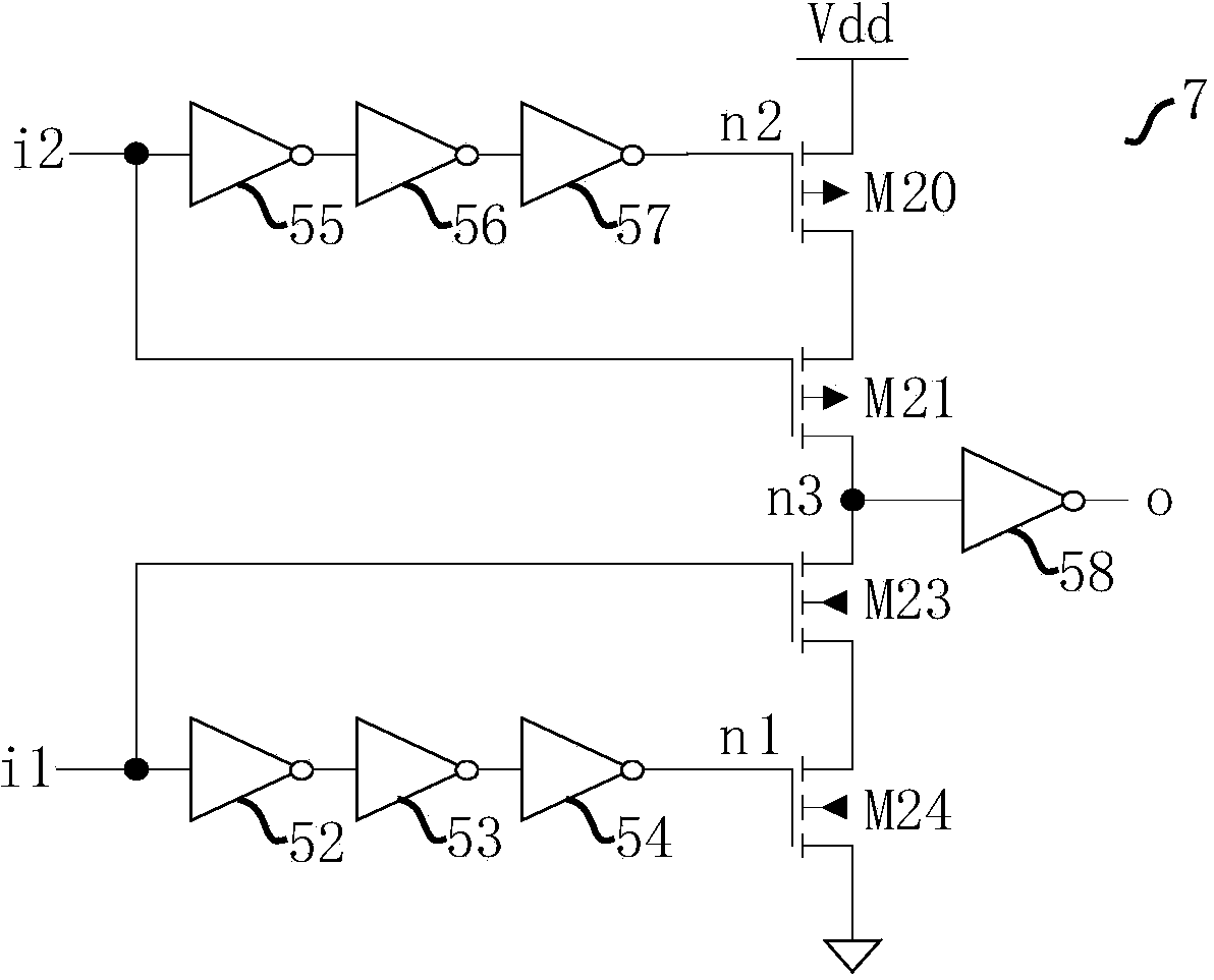
[0045] Figure 7 The block diagram of the high-speed ADC clock generation circuit provided by the embodiment of the present invention. Such as Figure 7 As shown, the entire ADC circuit is composed of a sample-and-hold circuit 6 , a quantizer 4 , and a clock generation circuit 5 . The sample and hold circuit 6 performs tracking sampling and holding on the analog input Vi to obtain the held voltage Vh, and the quantizer 4 performs quantization conversion on the voltage Vh to obtain the A / D conversion digital output Do. The clock generation circuit 5 is the core control module of the high-speed ADC, which provides the required control clock for the sample-and-hold circuit 6 and the quantizer 4 . The clock generation circuit 5 includes: a low-nois...


PUM


Abstract

The invention discloses a clock generation circuit used in an analog-to-digital converter (ADC) with a high speed and high precision. The clock generation circuit comprises: a low noise amplification and shaping circuit, a pulse width controller, a DLL with pulse width calibration, a biphase non-overlapping clock generation circuit and a clock buffer. A voltage-controlled delay line (VCDL) with pulse width adjustment is designed in the DLL with the pulse width calibration. The VCDL can realize clock signal time delay and pulse width control based on a cascade group comprising same M improvement delay units. The DLL with the pulse width calibration and the biphase non-overlapping clock generation circuit together form a time-delay control and pulse width adjustment loop. Therefore, working sequences of an ADC sampling circuit and a quantizer can be synchronized and stable processing to an input clock duty ratio can be realized. By using the technical scheme of the invention, a bandwidth requirement to an ADC driving circuit can be reduced; difficulty for designing the system and power consumption can be reduced; realization precision of the ADC quantizer can be improved.

Description

technical field [0001] The present invention relates to analog-to-digital converter technology, in particular to a clock generating circuit for high-speed and high-precision analog-to-digital converter. Background technique [0002] With the advent of the new generation of wireless communication era, the digital intermediate frequency receiver in the communication system puts forward higher requirements on the speed and accuracy of the analog-to-digital converter ADC, and the ADC presents a trend of high speed and high precision development. For high-speed and high-resolution ADCs, the quantizer is required to achieve high settling accuracy in a short period of time. Since the circuit in the quantizer is established in two phases alternately, it is required to control the work of the quantizer. The non-overlapping clocks have the same pulse width to optimize the operating speed of the entire quantizer. The higher the conversion speed of the ADC, the more demanding the settl...

Claims


Application Information

Patent Timeline
Patent Type & Authority Patents(China)
IPC IPC(8): H03M3/00
Inventor 李福乐赵晓晓张春
Owner TSINGHUA UNIV
Why Eureka
Eureka Blog
Learn More