Method for epitaxially growing type-II superlattice narrow-spectrum infrared photoelectric detector material

An epitaxial growth, electrical detector technology, applied in the direction of polycrystalline material growth, crystal growth, single crystal growth, etc., can solve problems such as increasing cost and reducing power consumption, and achieves reduction of dark current, improved performance, and high crystal quality. Effect

Inactive Publication Date: 2012-07-04
INST OF SEMICONDUCTORS - CHINESE ACAD OF SCI
View PDF1 Cites 34 Cited by
  • Summary
  • Abstract
  • Description
  • Claims
  • Application Information

AI Technical Summary

Problems solved by technology

Increases cost, detector weight, power consumption and reduces detector efficiency

Method used


Image

  • Method for epitaxially growing type-II superlattice narrow-spectrum infrared photoelectric detector material
  • Method for epitaxially growing type-II superlattice narrow-spectrum infrared photoelectric detector material
  • Method for epitaxially growing type-II superlattice narrow-spectrum infrared photoelectric detector material

Examples


Embodiment Construction

[0034] In order to make the object, technical solution and advantages of the present invention clearer, the present invention will be described in further detail below in conjunction with specific embodiments and with reference to the accompanying drawings.

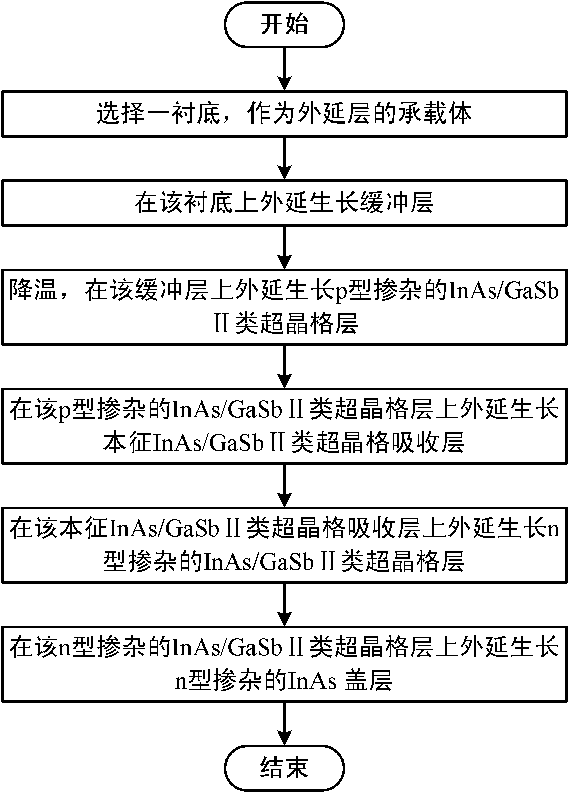
[0035] Such as figure 1 as shown, figure 1 It is a flow chart of a method for epitaxially growing InAs / GaSb II superlattice narrow-spectrum infrared photodetector material according to an embodiment of the present invention. The long-wave infrared detector is taken as an example to illustrate the method. The specific steps are as follows:

[0036] Step 1: Select a GaSb substrate 1 with a crystal orientation of (001), deoxidize it at 525° C. for 10-20 minutes under Sb atmosphere after baking, and remove the oxide on the surface of the GaSb substrate 1 as a carrier of the epitaxial layer.

[0037] Step 2: Lower the temperature of the GaSb substrate 1 to 500° C., and epitaxially grow a p-type GaSb buffer layer 2 with a thic...


PUM

PropertyMeasurementUnit
thicknessaaaaaaaaaa
thicknessaaaaaaaaaa
thicknessaaaaaaaaaa

Abstract

The invention discloses a method for epitaxially growing an InAs/GaSb type-II superlattice narrow-spectrum infrared photoelectric detector material. The method comprises the following steps of: selecting a substrate as a supporting body of an epitaxial layer; epitaxially growing a buffer layer on the substrate; cooling, and epitaxially growing a p-type doped InAs/GaSb type-II superlattice layer on the buffer layer; epitaxially growing an intrinsic InAs/GaSb type-II superlattice absorbing layer on the p-type doped InAs/GaSb type-II superlattice layer; epitaxially growing an n-type doped InAs/GaSb type-II superlattice layer on the intrinsic InAs/GaSb type-II superlattice absorbing layer; and epitaxially growing an n-type doped InAs cover layer on the n-type doped InAs/GaSb type-II superlattice layer to finish the epitaxial growth of the InAs/GaSb type-II superlattice narrow-spectrum infrared photoelectric detector material.

Description

technical field [0001] The invention relates to the technical field of growth of semiconductor infrared photodetector materials, in particular to an epitaxial growth method of InAs / GaSb II superlattice narrow-spectrum infrared photodetector materials. Background technique [0002] Infrared detectors are widely used in military and civil fields such as early warning, night vision, missile detection, temperature measurement, gas detection, meteorology, atmospheric monitoring, and medicine. The traditional mercury cadmium telluride detector (MCT) has excellent detection performance in the medium wave band and has been very mature. However, as the wavelength becomes longer, the difficulty of its material increases sharply, and it encounters challenges in the long-wavelength and very long-wavelength bands. [0003] Although quantum well infrared detector (QWIP) can realize the detection of narrow spectrum, QWIP is a transition between subbands, and its quantum efficiency is low; ...

Claims


Application Information

Patent Timeline
Patent Type & Authority Applications(China)
IPC IPC(8): C30B23/02C30B25/18C30B28/12C30B28/14C30B29/40H01L31/18
CPCY02P70/50
Inventor 张艳华马文全曹玉莲
Owner INST OF SEMICONDUCTORS - CHINESE ACAD OF SCI
Why Eureka
Try Eureka