SCR (Silicon Controlled Rectifier) structure for providing ESD ( Electro-Static discharge) protection for I/O (Input/Output) port of integrated circuit under all modes

An ESD protection and integrated circuit technology, applied in the electronic field, can solve the problems of increased primary breakdown voltage, increased on-resistance, and increased voltage of devices, and achieves the effects of ESD protection, small parasitic capacitance, and high efficiency

Inactive Publication Date: 2012-07-04
UNIV OF ELECTRONIC SCI & TECH OF CHINA
View PDF4 Cites 12 Cited by
  • Summary
  • Abstract
  • Description
  • Claims
  • Application Information

AI Technical Summary

Problems solved by technology

The disadvantage of this structure is that the series structure will increase the primary breakdown voltage of the device and increase the total on-resistance, which means increased power consumption and may lead to a decrease in ESD resistance
At the same

Method used


Image

  • SCR (Silicon Controlled Rectifier) structure for providing ESD ( Electro-Static discharge) protection for I/O (Input/Output) port of integrated circuit under all modes
  • SCR (Silicon Controlled Rectifier) structure for providing ESD ( Electro-Static discharge) protection for I/O (Input/Output) port of integrated circuit under all modes
  • SCR (Silicon Controlled Rectifier) structure for providing ESD ( Electro-Static discharge) protection for I/O (Input/Output) port of integrated circuit under all modes

Examples


specific Embodiment approach 1

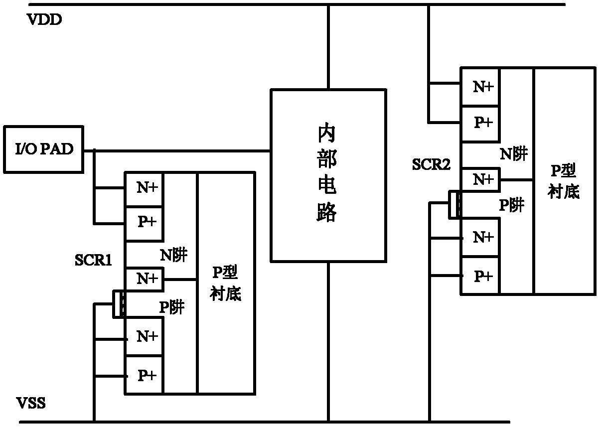
[0031] An SCR structure that provides full-mode ESD protection for integrated circuit I / O ports, such as Figure 4 As shown, it includes one P well region, two N well regions, three P+ regions and five N+ regions located on the substrate surface, and the P well region is sandwiched between two N well regions; the first N well region The middle of the top is the first P+ region, the top of the first N well region away from the P well region is the first N+ region; the middle of the top of the second N well region is the second P+ region, and the top of the second N well region is far away from the P well region One side of the top of the P well region is the second N+ region; the middle of the top of the P well region is the third N+ region on the side close to the first N well region, and the middle of the top of the P well region is the third P+ region on the side close to the second N well region; the fourth N+ The region is located in the region where the top of the first N...

specific Embodiment approach 2

[0032] Such as Figure 5 shown in Figure 4 On the basis of the technical solution shown, a sixth N+ region is added between the third P+ region and the second polysilicon region on the top of the P well region, which is close to the second N well region, and the first and second polysilicon regions are The crystal silicon region, the third and sixth N+ regions and the third P+ region are all connected to the VSS rail in the dual power rails of the protected integrated circuit chip through metal wires.

specific Embodiment approach 3

[0033] Such as Image 6 shown in Figure 4 On the basis of the technical solution shown, the third N+ region and the third P+ region are taken as a whole and rotated 90 degrees to the left or right in a manner parallel to the surface of the entire SCR structure, so that the third N+ region and the third P+ region are formed along the device The parallel arrangement in the length direction is changed to parallel and staggered arrangement along the width direction of the device (such as Image 6 (b) shown); and the first and second polysilicon regions, the third N+ region, and the third P+ region are all connected to the VSS rail in the power supply double rail of the protected integrated circuit chip through metal wires.


PUM


Abstract

The invention provides an SCR (Silicon Controlled Rectifier) structure for providing ESD (Electro-Static discharge) protection for an I/O (Input/Output) port of an integrated circuit under all modes, belonging to the technical field of electronics. The SCR structure comprises a P well region on the surface of a substrate, two N well regions, three P+ regions and five N+ regions. The P well region is sandwiched between the two N well regions; the first N+ region and the first P+ region are located in the first N well region and are connected with the I/O port of an external chip; the second N+ region and the second P+ region are located in the second N well region and are connected with a VDD (Voltage Drain Drain) track of a power source of the external chip; the third N+ region and the third P+ region are located in the P well region and are connected with a VSS (Voltage Series Series) track of the power source of the external chip; the fourth N+ region is located at the joint area of the first N well region and the top of the P well region; the fifth N+ region is located at the joint area of the P well region and the top of the second N well region; and a first and a second polysilicon regions are located on the surface of the P well region and are connected with the VSS track of the power source of the external chip. According to the invention, one single device is utilized to provide ESD protection for the I/O port under all modes, the occupying area of the protected device in the chip is effectively reduced and the parasitic capacitance is effectively reduced.

Description

technical field [0001] The invention belongs to the field of electronic technology, and relates to an electrostatic discharge (ElectroStatic Discharge, referred to as ESD) protection circuit design technology for semiconductor integrated circuit chips, especially a kind of SCR that provides full-mode ESD protection for integrated circuit input and output (I / O) ports (Silicon Controlled Rectifier) ​​structure. Background technique [0002] Electrostatic Discharge (ESD) phenomenon is the most important reliability problem that causes the failure of integrated circuit products. Studies have shown that 30% of integrated circuit failure products are caused by electrostatic discharge. Therefore, it is necessary to improve the protection of integrated circuits against electrostatic discharge. The reliability of the product has a non-negligible effect on improving the product yield and promoting the economic development of the industry. Electrostatic discharge will occur in a serie...

Claims


Application Information

Patent Timeline
IPC IPC(8): H01L27/02H02H9/02
Inventor 张波樊航蒋苓利吴道训何川
Owner UNIV OF ELECTRONIC SCI & TECH OF CHINA
Why Eureka
Try Eureka