Drawing method of thin film solar cell and thin film solar cell device

A technology for solar cells and scribing equipment, applied in welding equipment, laser welding equipment, metal processing equipment, etc., can solve the problem of high cost, achieve simple production methods, improve conversion efficiency, and reduce the effect of dead zone area

Active Publication Date: 2012-07-04
ZHEJIANG SHANGFANG ELECTRONICS EQUIP
View PDF4 Cites 8 Cited by
  • Summary
  • Abstract
  • Description
  • Claims
  • Application Information

AI Technical Summary

Problems solved by technology

[0002] Laser scribing is widely used in the production of thin-film solar cell modules. By using laser scribing, multiple cells can be formed on a single substrate and connected in series to form a battery module. The traditional process usually uses 3 laser scribing P1, P2 and P3 , where P1 is used for laser scribing of TCO, followed by semiconductor coating, then P2 is used for laser scribing of semiconductor film, then back electrode coating, and then P3 is used for back electrode laser scribing. The traditional process P1, P2 and P3 respectively require a One scribing equipment, the cost is higher

Method used


Image

  • Drawing method of thin film solar cell and thin film solar cell device
  • Drawing method of thin film solar cell and thin film solar cell device
  • Drawing method of thin film solar cell and thin film solar cell device

Examples


Embodiment 1

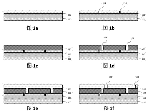
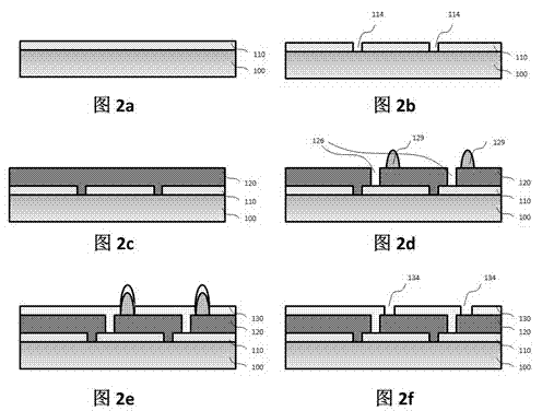
[0031] figure 2 Series is a schematic diagram of the laser scribing method for thin film solar cells of the present invention. figure 2 a is a substrate 100 with a transparent oxide TCO film layer 110, which is subjected to the first laser scribing P1 to form a TCO groove 114 ( figure 2 b), then cleaning the glass substrate 100, and then coating the semiconductor film 120 on the scribed TCO film layer 110 ( figure 2 c).

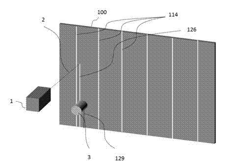
[0032] when using image 3 In the scribing equipment shown, the glass substrate 100 is subjected to two scribing lines P2 and P3 at the same time, and the laser scribing line P2 penetrates the semiconductor film layer 120 to form a second groove 126, see figure 2 d; the inkjet printing head is used as a soluble line forming device to simultaneously print and form a soluble material line 129 on the other side of the second groove 126 as a third groove preparation layer, see figure 2 d.

[0033] Continue to plate the back electrode film layer 130 on ...

Embodiment 2

[0037] The laser scribing method is the same as the first embodiment. The difference is when using image 3 In the scribing equipment shown, the glass substrate 100 is first subjected to the second laser scribing line P2, and the laser scribing line P2 penetrates the semiconductor film layer 120 to form the second groove 126, see figure 2 d; After the second groove 126 is formed, the laser printing head serves as the soluble line forming device 3 to print and form the soluble material line 129 on the other side of the second groove 126 as the third groove preparation layer, see figure 2 d.

[0038]Continue to plate the back electrode film layer 130 on the semiconductor film layer 120, then use water or an organic solvent to clean to remove the soluble line preparation layer 129 and the back electrode material deposited on the soluble line preparation layer 129, so that the back electrode layer A third trench 134 is formed on the film 130 .

[0039] From Figure 4a and ...


PUM


Abstract

The invention relates to a drawing method, especially relates to a drawing method of a thin film solar cell and a thin film solar cell device. The drawing method comprises three drawing lines (P2, P3, P1). According to traditional technology, drawing is conducted on a transparent conductive oxide film layer by means of laser. The drawing line (P1) penetrates through the transparent conductive oxide film layer, forming a first groove, and the drawing of drawing lines (P2, P3) is conducted after a semiconductor is coated with a film and before a back electrode is coated with a film. The drawing line (P2) penetrates through the semiconductor film layer, forming a second groove, in parallel with the first groove. The drawing line (P3) is provided with a soluble line which is disposed on the semiconductor film layer and in parallel with the second groove by means of soluble materials, and the soluble line is used as a preparation layer. The drawing device of the thin film solar cell combines a laser drawing device and a soluble line forming device on the same mechanical platform. The drawing device of the thin film solar cell has simple producing technology, low cost and can better cell performance and have long-term stability.

Description

technical field [0001] The invention relates to a laser scribing technology, in particular to a laser scribing method and equipment for the production of thin-film solar cells. Background technique [0002] Laser scribing is widely used in the production of thin-film solar cell modules. By using laser scribing, multiple cells can be formed on a single substrate and connected in series to form a battery module. The traditional process usually uses 3 laser scribing P1, P2 and P3 , where P1 is used for laser scribing of TCO, followed by semiconductor coating, then P2 is used for laser scribing of semiconductor film, then back electrode coating, and then P3 is used for back electrode laser scribing. The traditional process P1, P2 and P3 respectively require a Taiwan scribing equipment, the cost is higher. Contents of the invention [0003] One of the objectives of the present invention is to provide a method for scribing thin-film solar cells with accurate scribing positionin...

Claims


Application Information

Patent Timeline
Patent Type & Authority Applications(China)
IPC IPC(8): H01L31/18B23K26/36B23K26/364
CPCY02P70/50
Inventor 赵军梅芳
Owner ZHEJIANG SHANGFANG ELECTRONICS EQUIP
Why Eureka
Try Eureka