Phase change material for phase change storage and method for adjusting phase change parameter
A phase-change material and phase-change storage technology, applied in the field of optoelectronics, can solve problems such as limiting the process of practical development, and achieve the effect of information storage
- Summary
- Abstract
- Description
- Claims
- Application Information
AI Technical Summary
Problems solved by technology
Method used
Image
Examples
Embodiment 1
[0026] The electrical properties of phase change materials can be changed in a wide range. The change of the structural state of phase change materials will be accompanied by changes in electrical properties, and the range of change can reach multiple orders of magnitude. Voltage pulses can make phase change materials The reversible conversion between different structural states, and the information storage of phase change memory can be realized by using the change of electrical properties between different states.
[0027] By controlling Ge x SnTe or Si x The content of Ge and Si in SnTe can precisely adjust the crystallization temperature and melting point of the material. In an appropriate range, the material has a higher crystallization temperature and better reversible phase transition capability, and the memory based on the material has better performance.
[0028] Through the study of the resistivity of the material over time, it is found that the resistivity of the m...
Embodiment 2
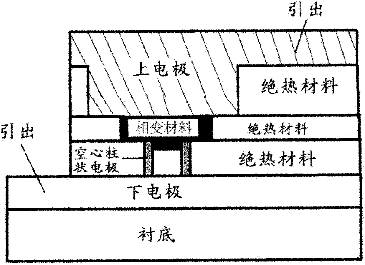
[0037] In order to test Ge x The electrical properties of SnTe-based storage materials, such as figure 2 The storage cell structure of the phase change memory is shown. The storage material is Ge 1.7 SnTe thin film material, the storage unit is completed by a standard semiconductor process line of 0.18 microns, and the dimensions of each film layer are as follows: the lower electrode is AI, and the film thickness is 300 nanometers; the heat insulating material layer on the lower electrode is SiO2 , and its thickness is 700 nanometers; the hollow columnar electrode in the insulating material SiO2 layer is W, its outer diameter is 260 nanometers, and its inner diameter is 100 nanometers; the insulating material layer on the hollow cylindrical electrode is SiO 2 , with a thickness of 200 nm; Ge 1.7 The thickness of the SnTe memory material is 150 nm; the Ge 1.7 The transition layer material on the SnTe storage material is TiN, and its thickness is 20 nanometers.
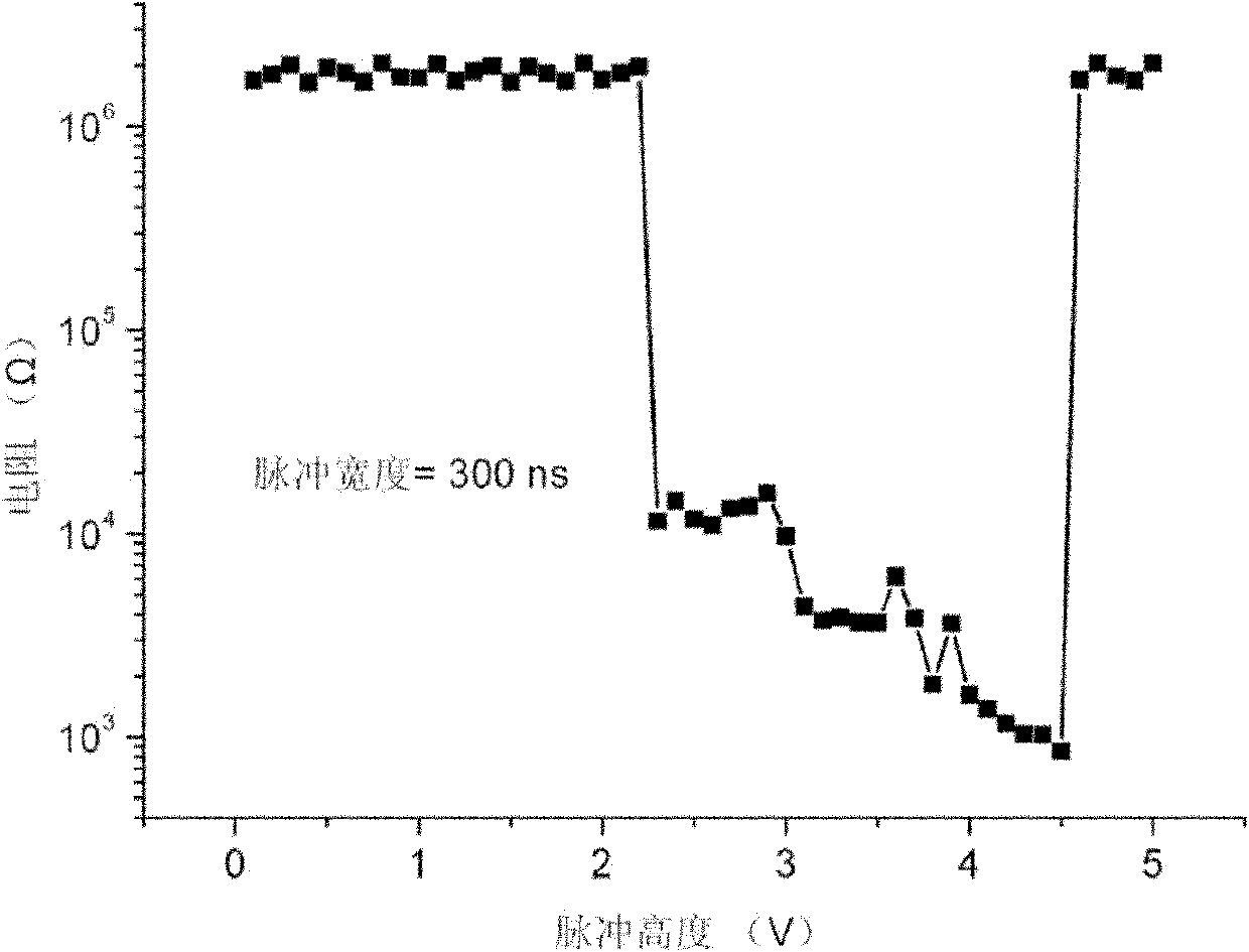
[0038] Per...
Embodiment 3
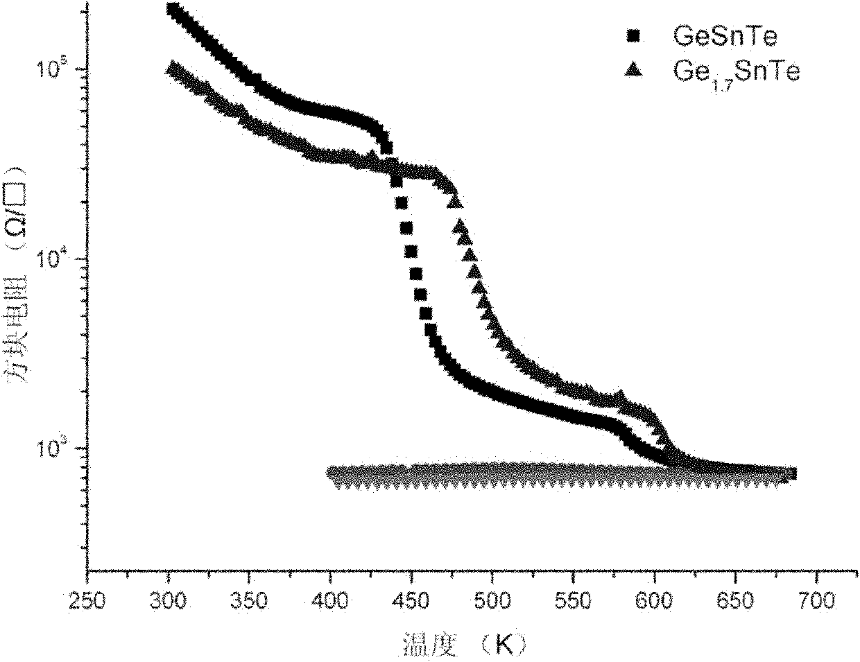
[0042] Preparation of Ge on thermally oxidized silicon substrates by magnetron sputtering 1.7 For SnTe and GeSnTe films, the film is heated in situ in a vacuum chamber with a vacuum degree of 10mtorr, and the sheet resistance change of the film is measured by a probe in the vacuum chamber that is in contact with the surface of the film. image 3 Display Ge 1.7 The resistance of both SnTe and GeSnTe decreases with the increase of temperature, and the resistance decreases rapidly and greatly at the crystallization temperature, with a difference of about two orders of magnitude. Ge 1.7 The crystallization temperature of SnTe is 477K, and that of GeSnTe is 447K. The increase of Ge content can improve the Ge x The crystallization temperature of SnTe material increases Ge x The thermal stability of SnTe makes Ge x SnTe retains data longer at higher temperatures.
PUM
| Property | Measurement | Unit |
|---|---|---|
| thickness | aaaaa | aaaaa |
| thickness | aaaaa | aaaaa |
| thickness | aaaaa | aaaaa |
Abstract
Description
Claims
Application Information


