
Phase change material for phase change memory and preparation method thereof

A phase-change memory and phase-change material technology, applied in the field of microelectronics, can solve problems such as poor data retention, low crystallization temperature, and slow phase change speed, achieve phase change speed and fatigue cycle characteristics, and realize information storage Effect

Active Publication Date: 2020-05-05
SHANGHAI INST OF MICROSYSTEM & INFORMATION TECH CHINESE ACAD OF SCI
View PDF4 Cites 0 Cited by
  • Summary
  • Abstract
  • Description
  • Claims
  • Application Information

AI Technical Summary

Problems solved by technology

[0007] In view of the shortcomings of the prior art described above, the purpose of the present invention is to provide a phase change material for phase change memory and its preparation method, which is used to solve the problems of low crystallization temperature and thermal stability of the phase change material in the prior art. Low performance, poor data retention and slow phase transition

Method used


Image

  • Phase change material for phase change memory and preparation method thereof
  • Phase change material for phase change memory and preparation method thereof
  • Phase change material for phase change memory and preparation method thereof

Examples


Embodiment 1

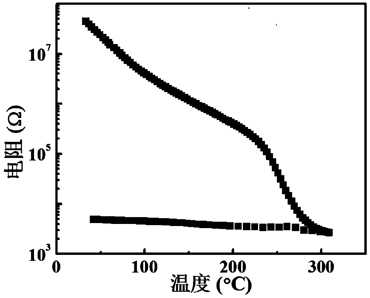
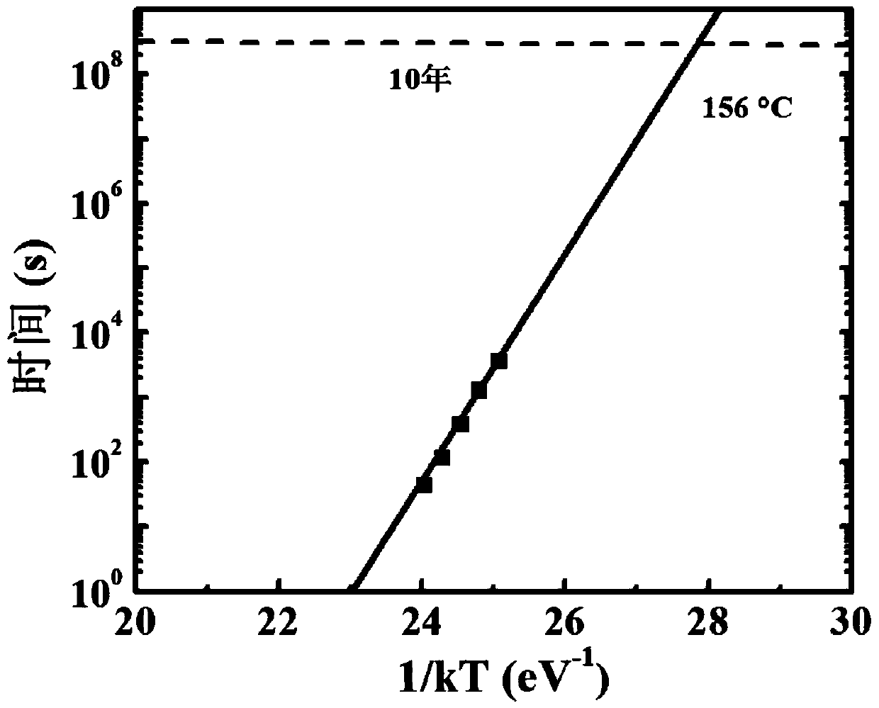
[0032] This embodiment provides a Sc for phase change memory 100-x-y-z Ge x Sb y Te z Phase change material system, wherein, the phase change material system is in Sb 2 Te 3 It is formed by doping Sc on the basis of the phase change material system, and its general chemical formula is Sc 100-x-y- z Ge x Sb y Te z , where x=0, 0

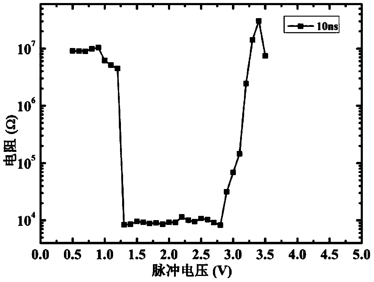
[0033] The phase change material realizes reversible phase transition through electric drive, laser pulse drive or electron beam drive, and realizes the function of data storage.

[0034] Specifically, in this embodiment, the Sc 100-x-y-z Ge x Sb y Te z The general chemical formula of phase change materials is Sc 5 Sb 38 Te 57 , and using Sb 2 Te 3 Co-sputtering of alloy target and Sc elemental target to obtain Sc 5 Sb 38 Te 57 For thin films, different thicknesses of materials can be controlled by controlling the sputtering time. In this embodiment, sputtering is under 99.999% argon atmosphere, Sb 2 Te 3 The alloy target...

Embodiment 2

[0040] This embodiment adopts basically the same technical solution as Embodiment 1, the difference is that the Sb in Embodiment 1 2 Te 3 Alloy target changed to Sb 2 Te alloy target. The remaining steps are exactly the same as in Example 1. The electrical properties of the obtained corresponding devices can also achieve similar effects.

Embodiment 3

[0042] This embodiment provides a Sc for phase change memory 100-x-y-z Ge x Sb y Te z A phase change material system, wherein the phase change material system is a structure Sc 2 Te 3 -Sb 2 Te 3 Pseudo binary phase change material system, its chemical formula is Sc 100-x-y- z Ge x Sb y Te, where x=0, 0

[0043] The phase change material realizes reversible phase transition through electric drive, laser pulse drive or electron beam drive, and realizes the function of data storage.

[0044] Specifically, in this embodiment, the Sc 100-x-y-z Ge x Sb y Te z The general chemical formula of phase change materials is Sc 20 Sb 20 Te 60 , and adopt the co-sputtering method of Sc simple substance target, Sb simple substance target and Te simple substance target to obtain Sc 20 Sb 20 Te 60 For thin films, different thicknesses of materials can be controlled by controlling the sputtering time. In this embodiment, the sputtering is carried out under a 99.999% arg...


PUM

PropertyMeasurementUnit
thicknessaaaaaaaaaa

Abstract

The invention provides a phase change material used in a phase change memory and a preparation method thereof. The general chemical formula of the phase change material used in a phase change memory is Sc 100‑x‑y‑z Ge x Sb y Te z , wherein, 0≤x≤60, 0≤y≤90, 0<z≤65, 0<100-x-y-z<100. The phase change material that can be used for phase change storage of the present invention has the ability of repeated phase change; Sc 100‑x‑y‑z Ge x Sb y Te z It has two different resistance states of high resistance and low resistance, and the reversible conversion between the high resistance state and the low resistance state can be realized by applying a pulse electric signal, which meets the basic requirements of phase change memory storage materials. It is a new type of storage material; the thermal stability, phase change speed and fatigue cycle characteristics of the material have been improved; pulse voltage or pulse laser can be used to drive the phase change material to undergo reversible transition between different structural states, and at the same time make the performance of the phase change material A reversible change occurs, thereby realizing the information storage of the phase change memory.

Description

technical field [0001] The invention belongs to the field of microelectronics, and relates to a phase change material Sc used for a phase change memory 100-x-y-z Ge x Sb y Te z and its preparation method. Background technique [0002] The development of information storage technology is the embodiment of the progress of human civilization. From the invention of the transistor to the advent of the integrated circuit, mankind ushered in a glorious information age. The rapid development of information technology promotes the rapid development of storage technology towards non-volatility, high speed, low operating power consumption and good cycle characteristics. As the current mainstream non-volatile storage technology, flash memory has been widely used. However, with the rapid development of integrated circuits, the shortcomings of flash memory such as limited cycle times, slow operating speed, and high operating voltage limit its further application. Therefore, seeking...

Claims


Application Information

Patent Timeline
Patent Type & Authority Patents(China)
IPC IPC(8): H01L45/00H01L27/24G11C13/00
CPCG11C13/00H10B63/00H10N70/00G11C13/0004H10N70/231H10N70/026H10N70/8828H10N70/023
Inventor 丁科元饶峰王勇宋志棠
Owner SHANGHAI INST OF MICROSYSTEM & INFORMATION TECH CHINESE ACAD OF SCI
Learn More