Manufacture method of metal grid electrode

A technology of metal gate and manufacturing method, which is applied in semiconductor/solid-state device manufacturing, electrical components, semiconductor devices, etc., can solve problems affecting and affecting the performance of semiconductor devices, and achieve the effect of eliminating the step effect

Active Publication Date: 2012-07-11
SEMICON MFG INT (SHANGHAI) CORP +1
View PDF5 Cites 1 Cited by
  • Summary
  • Abstract
  • Description
  • Claims
  • Application Information

AI Technical Summary

Problems solved by technology

[0023] It can be seen from the above scheme of making metal gates that due to Image 6 The steps shown will affect the subsequent etchin

Method used


Image

  • Manufacture method of metal grid electrode
  • Manufacture method of metal grid electrode
  • Manufacture method of metal grid electrode

Examples


Embodiment Construction

[0043] In order to make the objectives, technical solutions and advantages of the present invention clearer, the present invention will be further described in detail below with reference to the accompanying drawings and embodiments.

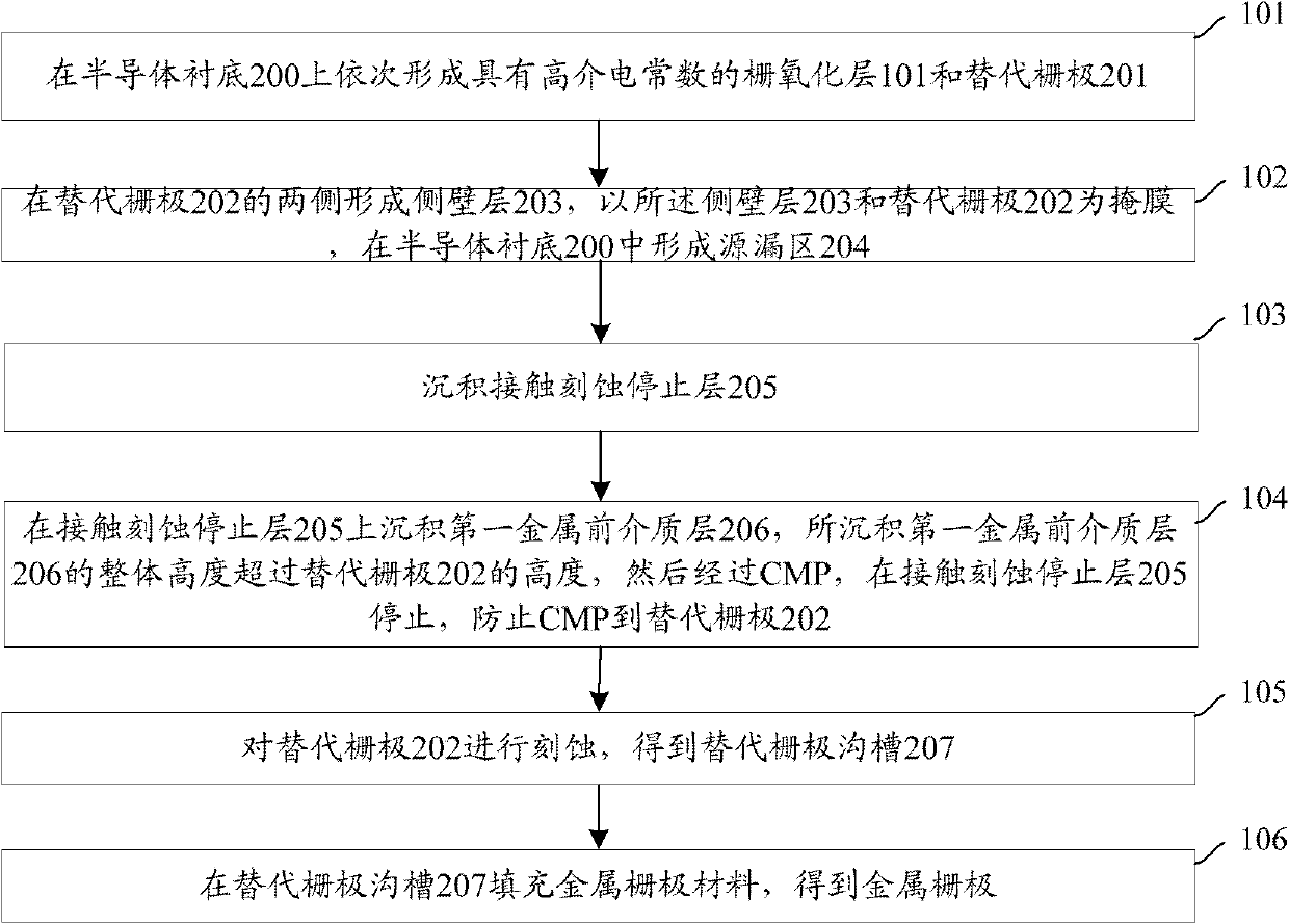
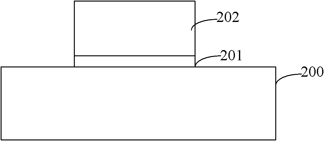
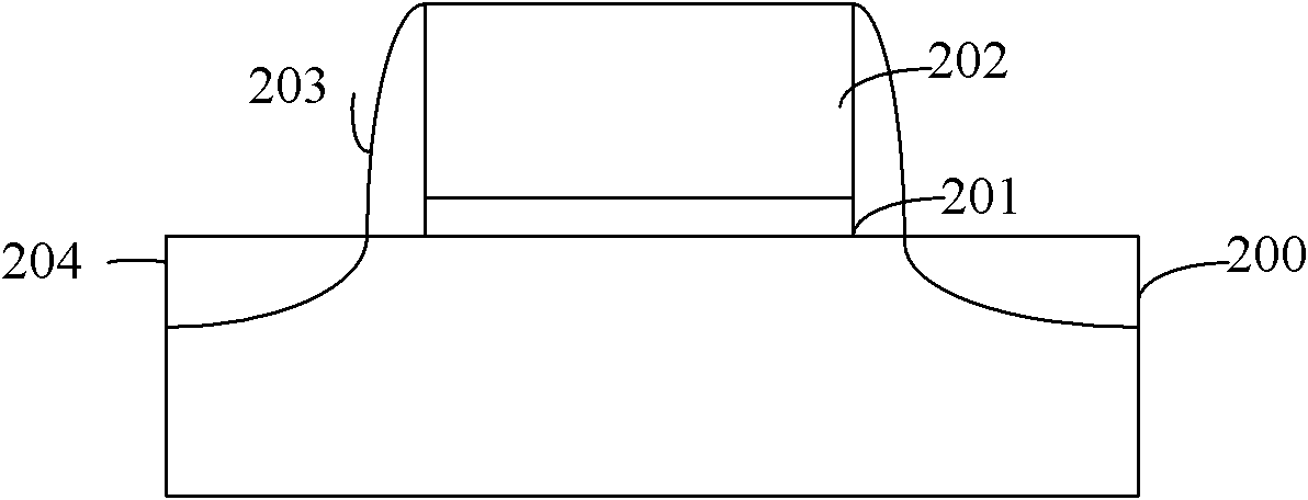
[0044] In the process of making the metal gate, in order to overcome the step effect on the semiconductor device when the first pre-metal dielectric layer is polished, the present invention, before etching the replacement gate, after polishing the first pre-metal dielectric layer, It also includes depositing a second pre-metal dielectric layer to cover the steps produced by polishing the first pre-metal dielectric, and then polishing the second pre-metal dielectric layer to the surface of the replacement gate. In this way, during subsequent etching of the replacement gate and filling of the metal gate, there will be no steps on the semiconductor device.

[0045] In the present invention, the second pre-metal dielectric may be a silicon oxide layer, w...


PUM


Abstract

A manufacture method of a metal grid electrode comprises forming a gate oxide and a substitution grid electrode on a provided semiconductor substrate and then forming lateral wall layers on two sides of the substitution grid electrode; considering the lateral wall layers and the substitution grid electrode as masks and conducting ion implantation on the semiconductor substrate to form a source and drain region; depositing a contact etching stopping layer on the surfaces of the semiconductor substrate, the lateral wall layers and the substitution grid electrode; depositing a first metal front medium layer on the contact etching stopping layer, enabling the height of the deposited first metal front medium layer to be higher than the surface of the substitution grid electrode, polishing to reach the first metal front medium layer, and forming footsteps on the surfaces of the contact etching stopping layer and the first metal front medium layer which are in a same plane; depositing a second metal front medium layer on the surfaces of the first metal front medium layer and the contact etching stopping layer, completely covering the footsteps, polishing again to reach the substitution grid electrode; and etching the substitution grid electrode to obtain a substitution grid electrode channel and filling the metal grid electrode in the substitution grid electrode channel. The manufacture method removes the footstep effect produced in a manufacture process.

Description

Technical field [0001] The present invention relates to detection technology in the semiconductor field, in particular to a manufacturing method of a metal gate. Background technique [0002] At present, high dielectric constant insulating materials and metal gates will be used to manufacture logic circuit devices in semiconductor devices. [0003] In order to control the short channel effect, semiconductor devices with smaller feature sizes require further increase in gate electrode capacitance. This can be achieved by continuously reducing the thickness of the gate oxide layer, but the subsequent increase in the leakage current of the gate electrode. When silicon dioxide is used as the gate oxide layer and the thickness is less than 3.0 nanometers, the leakage current becomes intolerable. The solution to the above problems is to use high-dielectric constant insulating materials instead of silicon dioxide. High-dielectric constant insulating materials can be hafnium silicate, ha...

Claims


Application Information

Patent Timeline
IPC IPC(8): H01L21/28H01L21/283
Inventor 鲍宇蒋莉
Owner SEMICON MFG INT (SHANGHAI) CORP
Why Eureka
Try Eureka