Detection method of semiconductor device defect

A detection method, a semiconductor technology, applied in the direction of semiconductor/solid-state device testing/measurement, optical testing flaws/defects, etc., can solve problems such as yield decline, failure to remedy in time, semiconductor device defects, etc., to improve yield and quality , The effect of reducing the waste rate

Active Publication Date: 2012-07-11
CSMC TECH FAB2 CO LTD
View PDF7 Cites 20 Cited by
  • Summary
  • Abstract
  • Description
  • Claims
  • Application Information

AI Technical Summary

Problems solved by technology

[0005] The problem solved by the present invention is a method for detecting defects of semiconductor devices, preventing defects from being remedied in time, resulting in a decrease in yield

Method used


Image

  • Detection method of semiconductor device defect
  • Detection method of semiconductor device defect
  • Detection method of semiconductor device defect

Examples


Embodiment Construction

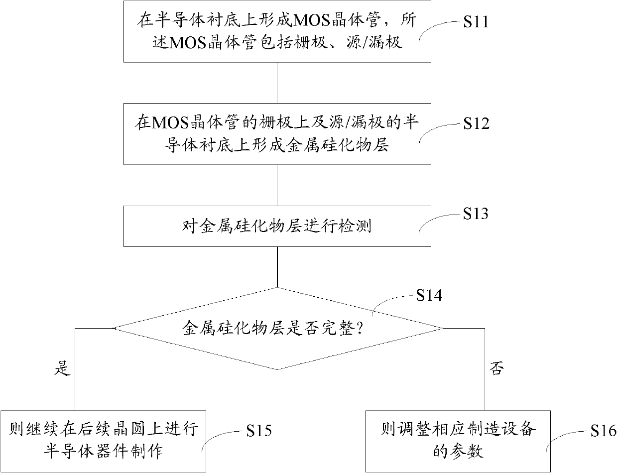
[0019] The inventor's existing inspection process is usually after the semiconductor device is fabricated on the wafer, in the quality inspection stage or when the finished product is sent to the customer, the quality inspector or customer can determine the defects in the semiconductor device by conducting electrical tests on the finished product For example, the production of TEM test samples is usually after all semiconductor devices are fabricated on the wafer, and then the isolation structure is electrically tested. If any abnormality is found, the abnormality is located, and then cutting is performed. Determine if the defect is at the location and the size of the defect. As a result, defects cannot be remedied in time, resulting in a decrease in yield, excessive waste, and great risks to the production of subsequent wafers in the mass-produced production line.

[0020] Therefore, the inventor found through research that if the semiconductor device is produced on the produ...


PUM


Abstract

The invention discloses a detection method of a semiconductor device defect. The method comprises the following steps of: forming an MOS (Metal Oxide Semiconductor) transistor on a semiconductor substrate, wherein the MOS transistor comprises a grid and a source/drain; forming a metal silicide layer on the semiconductor substrate on the grid and the source/drain of the MOS transistor; detecting the metal silicide layer; and continually manufacturing the semiconductor device on a subsequent wafer if no defect is detected, and adjusting parameters of corresponding manufacturing equipment if a certain requirement is not met. According to the detection method, the situation of waste of a large batch of wafers caused by detection after manufacturing of a finished product is avoided, and the yield is increased while wastage rate is lowered.

Description

technical field [0001] The invention relates to the field of semiconductor detection, in particular to a detection method for semiconductor device defects. Background technique [0002] As the size of integrated circuits decreases, the devices that make up the circuits must be placed more densely to fit the limited space available on the chip. As devices continue to get smaller, their critical dimensions and film thickness are becoming more and more difficult to control. Therefore, control of thin film and device integrity (GOI) is very important in IC manufacturing. [0003] In the prior art, because the tape-out period of the product is long (generally more than 45 days), if the film layer or the device is defective, it will cause a great impact. At present, in the semiconductor manufacturing industry, there are various detection equipment, such as SEM (Scan Electron Microscope, scanning electron microscope), TEM (Transmission Electron Microscope, transmission electron m...

Claims


Application Information

Patent Timeline
Patent Type & Authority Applications(China)
IPC IPC(8): H01L21/66G01N21/95
Inventor 陈亚威
Owner CSMC TECH FAB2 CO LTD
Why Eureka
Try Eureka