
Manufacturing method of static random access memory

A manufacturing method, static random technology, applied in semiconductor/solid-state device manufacturing, electrical components, circuits, etc., can solve problems such as low yield rate of static random access memory, electrical incompatibility between NMOS devices and PMOS devices, and reduce the distance , Improve the effect of yield rate

Active Publication Date: 2012-07-11
SEMICONDUCTOR MANUFACTURING INTERNATIONAL (BEIJING) CORP
View PDF6 Cites 1 Cited by
  • Summary
  • Abstract
  • Description
  • Claims
  • Application Information

AI Technical Summary

Problems solved by technology

[0005] However, with the continuous reduction of the process node of semiconductor devices, the requirements for the manufacturing process of semiconductor devices are becoming more and more stringent. The NMOS devices and PMOS devices in the static random access memory devices manufactured by the existing technology are electrically incompatible, resulting in the manufacture of static random access memory devices. Memory yield is low

Method used


Image

  • Manufacturing method of static random access memory
  • Manufacturing method of static random access memory
  • Manufacturing method of static random access memory

Examples


Embodiment Construction

[0021] In order to make the above objects, features and advantages of the present invention more comprehensible, specific implementations of the present invention will be described in detail below in conjunction with the accompanying drawings.

[0022] In the following description, many specific details are set forth in order to fully understand the present invention, but the present invention can also be implemented in other ways than those described here, so the present invention is not limited by the specific embodiments disclosed below.

[0023] As mentioned in the background technology section, the existing SRAM manufacturing process mainly changes the conditions of gate secondary oxidation, the thickness of the sidewall of silicon nitride, the energy of ion implantation, and the etching process in the process of manufacturing semiconductor devices. The problem of incompatibility between devices in the manufactured SRAM is improved, but the improvement effect of these meth...


PUM


Abstract

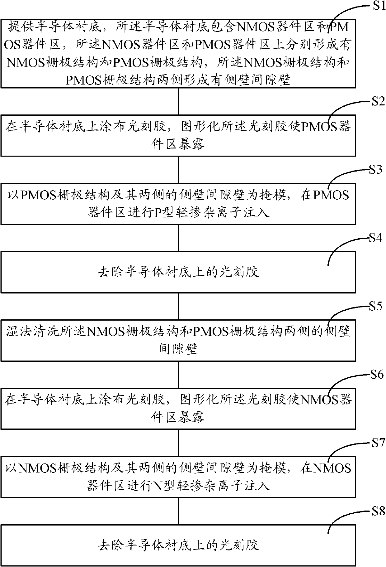
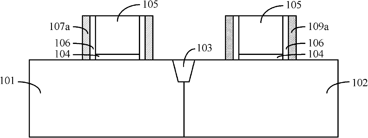
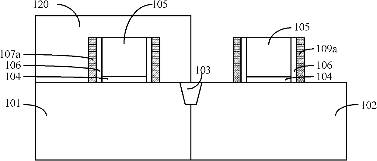
A manufacturing method of a static random access memory is disclosed. The static random access memory simultaneously comprises an N-type metal oxide semiconductor (NMOS) device and a P-type metal oxide semiconductor (PMOS) device. By wet cleaning of the gap wall of the side walls of the NMOS device and the PMOS device in the static random access memory after performing lightly-doped ion implantation on a source / drain of the PMOS device, a distance between a source lightly-doped region and a drain lightly-doped region of the NMOS device formed after wet cleaning is decreased, electrical properties of the NMOS device are improved to be matched with electrical properties of the PMOS device in the static random access memory, and the yield of static random access memories is increased.

Description

technical field [0001] The present invention relates to the technical field of semiconductors, and more specifically, the present invention relates to a method for manufacturing a SRAM. Background technique [0002] With the continuous development of modern high-tech industries represented by electronic communication technology, the total output value of the world's integrated circuit industry is growing at a rate of 30% every year. Static random access memory is an important component in integrated circuits, with small size and high density. Among semiconductor memory devices, Static Random Access Memory (SRAM) has advantages of lower power consumption and faster operation speed than Dynamic Random Access Memory (DRAM) devices. Static random access memory can easily locate the physical unit through the bitmap test equipment to study the effective mode of the product. In addition, the yield rate of the SRAM can be used as an important index to measure the yield rate of the...

Claims


Application Information

Patent Timeline
Patent Type & Authority Applications(China)
IPC IPC(8): H01L21/8244H01L21/02H01L21/336H10B10/00
Inventor 刘焕新宋伟基
Owner SEMICONDUCTOR MANUFACTURING INTERNATIONAL (BEIJING) CORP
Learn More