PCM (phase change memory) and forming method thereof

A technology of phase-change memory and phase-change materials, which is applied in the field of phase-change memory and its formation, can solve the problems of poor film quality and poor doping concentration uniformity of buried layers, so as to improve device performance, improve film quality, and avoid damage effect

Inactive Publication Date: 2012-07-11
SEMICON MFG INT (SHANGHAI) CORP +1
View PDF6 Cites 1 Cited by
  • Summary
  • Abstract
  • Description
  • Claims
  • Application Information

AI Technical Summary

Problems solved by technology

[0008] The problem solved by the invention is that the film quality of the PN junction in the phase change memory is poor, and the doping concentration uniformity of the buried layer is poor

Method used


Image

  • PCM (phase change memory) and forming method thereof
  • PCM (phase change memory) and forming method thereof
  • PCM (phase change memory) and forming method thereof

Examples


Embodiment Construction

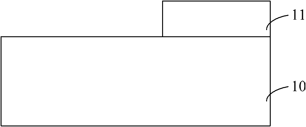
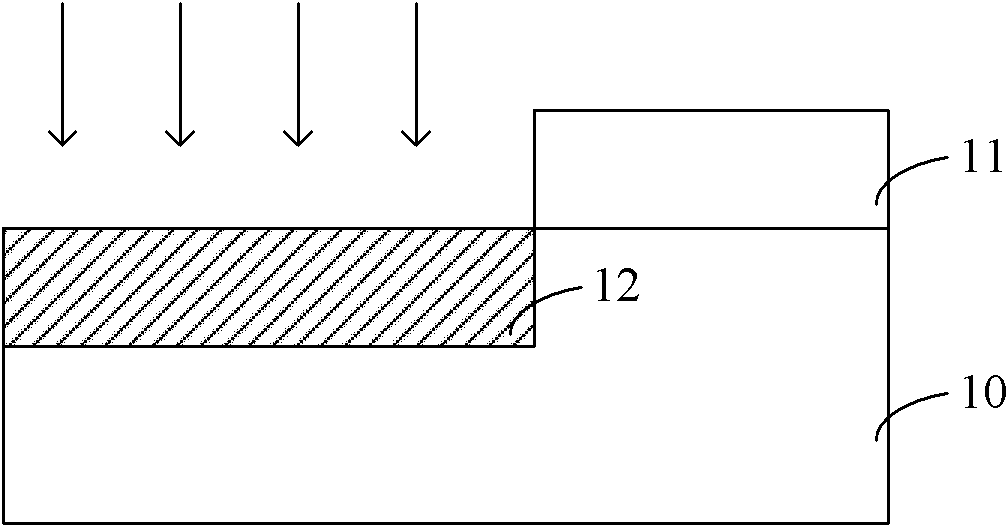
[0053] The existing technology uses ion implantation to form a buried layer in the semiconductor substrate as the word line of the phase change memory, but the process of ion implantation will cause damage to the surface of the semiconductor substrate, affecting the film quality of the PN junction subsequently formed on it. , resulting in degraded device performance.

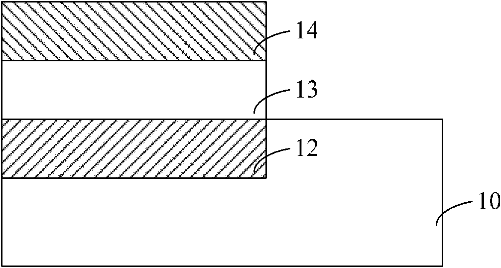
[0054]In the technical solution, a trench is formed on a semiconductor substrate, and then a first epitaxial layer is formed in the trench by epitaxial growth, and the first epitaxial layer is an N-type doped or P-type doped semiconductor material. The first epitaxial layer is used as the word line of the phase change memory, which is equivalent to the buried layer in the prior art. Since its formation process is formed by epitaxial growth, damage to the surface of the semiconductor substrate is avoided, which is conducive to improving the subsequent The film quality of other thin films formed on it, such as PN ...


PUM


Abstract

The invention provides a PCM (phase change memory) and a forming method thereof. The forming method of the PCM comprises the steps as follows: providing a semiconductor substrate, forming a groove on the semiconductor substrate, and forming epitaxy growth in the groove to form a first epilayer, which is an N-type doped semiconductor material or a P-type doped semiconductor material. According to the invention, the improvement on the film quality of a PN junction can be facilitated, the uniformity of doping concentration of the first epilayer serving as a word line is improved, and the problem of resistance increase of the word line can be avoided.

Description

technical field [0001] The invention relates to semiconductor technology, in particular to a phase change memory and a forming method thereof. Background technique [0002] Phase Change Memory (PCM, Phase Change Memory) is a new type of memory, and it is a non-volatile memory that is most likely to replace flash memory (Flash) at a 32nm process node. Its storage principle is that the phase change material undergoes a phase change and switches between a high-resistance state and a low-resistance state to realize the storage function. Generally, heat is generated by applying an electrical signal, so that the phase-change material is mutually converted between a low-resistance crystalline state and a high-resistance amorphous state. The most commonly used phase change materials are chalcogenides, especially germanium-antimony-tellurium (GST, Ge 2 Sb 2 Te 5 ). [0003] The phase-change memory in the prior art generally uses an N-type doped buried layer (NBL, N type BuriedLa...

Claims


Application Information

Patent Timeline
Patent Type & Authority Applications(China)
IPC IPC(8): H01L45/00
Inventor 三重野文健涂火金何有丰
Owner SEMICON MFG INT (SHANGHAI) CORP
Why Eureka
Try Eureka