Wafer-level vacuum encapsulated infrared focal plane array (IRFPA) device and method for producing same

A vacuum packaging, wafer-level technology, used in electrical radiation detectors, radiation control devices, etc., can solve the problems of reducing imaging quality, manufacturing, and high costs

Active Publication Date: 2012-07-25
中科芯未来微电子科技成都有限公司
View PDF3 Cites 46 Cited by
  • Summary
  • Abstract
  • Description
  • Claims
  • Application Information

AI Technical Summary

Problems solved by technology

This structure is manufactured on the silicon wafer that has completed the readout circuit. Since there is a relatively thick dielectric layer on the readout circuit silicon wafer, a large heat capacity is formed, and the infrared energy absorbed by the pixel cannot be dissipated in time. Going out will bring crosstalk between pixels, thereby reducing the image quality
figure 1 The VOx material in the IC is also incompatible with the IC process, so the structure cannot be manufactured in the IC factory, resulting in relatively high cost

Method used


Image

  • Wafer-level vacuum encapsulated infrared focal plane array (IRFPA) device and method for producing same
  • Wafer-level vacuum encapsulated infrared focal plane array (IRFPA) device and method for producing same
  • Wafer-level vacuum encapsulated infrared focal plane array (IRFPA) device and method for producing same

Examples


Embodiment 1

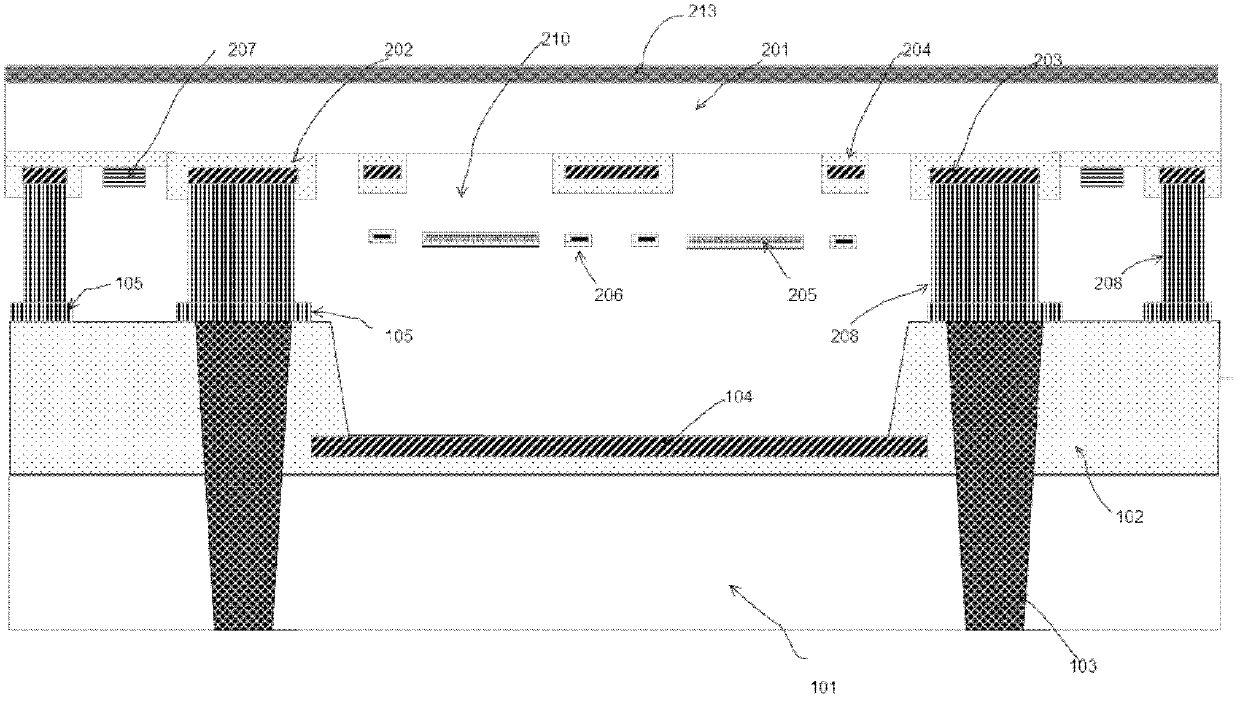
[0067] The structural sectional view of embodiment 1 of the present invention is as figure 2As shown, the first wafer 101 and the second wafer 201 are included. On the silicon substrate of the second wafer 201, the infrared focal plane array device is manufactured by photolithography and etching of the conventional IC process. microstructure. The specific structure is: the first wafer 101 is a conventional silicon wafer, and the readout circuit of the IR FPA is produced by using a conventional IC manufacturing process, and at the same time, the uppermost layer metal of the first wafer 101 is used to produce the IR FPA device. The resonant absorbing reflector 104; on the side of the first wafer 101 with the reflector 104, a dielectric material 102 is deposited, and a TSV structure 103 is formed through the first wafer 101 and the dielectric material 102 for electrical connection And to realize chip packaging, make the first low-temperature soldering material 105 at the electr...

Embodiment 2

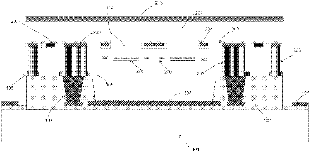
[0078] The structural sectional view of Embodiment 2 of the present invention is as image 3 As shown, the difference from Example 1 lies in the extraction of the last solder joint. The solder joint in Example 1 is extracted from the bottom of the first wafer by the method of TSV. Embodiment 2 is the readout of the first wafer. lead out around the circuit.

[0079] The specific structure is: the first wafer 101 is a conventional silicon wafer, and the readout circuit of the IR FPA is produced by using a conventional IC manufacturing process, and at the same time, the resonance required by the IR FPA device is produced by the uppermost metal of the first wafer 101 Absorbing reflector 104; a dielectric material 102 is deposited on one side of the first wafer 101 with reflector 104, and the dielectric material 102 includes a boss in the middle, and the periphery of the boss is lower than the middle to form an edge, and the boss A TSV structure 103 is formed inside, and a through...

Embodiment 3

[0089] The structural sectional view of embodiment 3 of the present invention is as Figure 4 As shown, its main structure is similar to that of Embodiment 1, the main difference is that the light-condensing integrated microlens is added, thereby increasing the filling factor of the structure and improving the performance of the device.

[0090] The difference in the main production steps is in the seventh step (such as Figure 9-7 As shown), before making the anti-reflection layer material 213, the micro-convex lens array or the Fresnel lens array is made by photolithography and etching, and then the anti-reflection layer material 213 is made to complete the manufacture of the entire device.


PUM


Abstract

The invention discloses a wafer-level vacuum encapsulated infrared focal plane array (IRFPA) device and a method for producing the same, wherein a double-wafer bonding mode is adopted to produce an infrared detector and realize the wafer-level encapsulation, a complementary metal-oxide-semiconductor integrated chip (CMOSIC) and a micro-electromechanical systems (MEMS) device are separately produced, so the integration of the CMOSIC is realized, the production flexibility of the MEMS infrared detector device is also increased, and the wafer-level encapsulation can be realized at the same time. The invention has the advantages that: a reflector for a complementary metal-oxide-semiconductor integrated chip (CMOS) reading circuit and a resonance absorption structure is produced on a wafer, the other wafer is utilized to produce the MEMS structural part of the IRFPA and is simultaneously used for producing the infrared window of the IRFPA, the resonance absorption structure is utilized to provide the infrared absorption efficiency of the infrared IRFPA device, the wafer-level encapsulation of the IRFPA device is also realized at the same time, so the size and the production cost of the IRFPA device are benefited to be reduced.

Description

technical field [0001] The invention relates to an IR FPA device and a manufacturing method thereof, in particular to an IR FPA device adopting wafer-level vacuum packaging and a manufacturing method thereof. Background technique [0002] Infrared imaging technology is widely used in military, industrial, agricultural, medical, forest fire prevention, environmental protection and other fields. Its core component is the Infrared Focal Plane Array (IRFPA). According to the classification of working principle, it can be divided into: photon infrared detector and uncooled infrared detector. Photon-type infrared detectors use narrow-bandgap semiconductor materials, such as HgCdTe, InSb, etc., and use the photoelectric effect to realize the conversion of infrared light signals into electrical signals; therefore, they need to work at a temperature of 77K or lower, which requires bulky and complicated Refrigeration equipment is difficult to miniaturize and inconvenient to carry. O...

Claims


Application Information

Patent Timeline
Patent Type & Authority Applications(China)
IPC IPC(8): H01L27/144G01J5/20
Inventor 欧文蒋文静
Owner 中科芯未来微电子科技成都有限公司
Why Eureka
Try Eureka