Weak correlation multiport parallel store controller
A storage controller and multi-port technology, applied in the direction of instruments, electrical digital data processing, input/output to record carrier, etc., can solve the problem of low processor frequency, multi-core processor and large-capacity L2 shared storage Unsuitable for occasions, low flexibility, etc., to achieve the effect of layout and wiring, simple structure, and high flexibility
- Summary
- Abstract
- Description
- Claims
- Application Information
AI Technical Summary
Problems solved by technology
Method used
Image
Examples
Embodiment 1
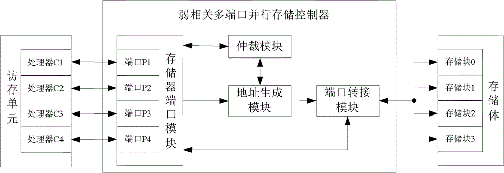
[0043] A weakly correlated multi-port parallel storage controller in this embodiment, its structural diagram is as follows figure 1 As shown, it is connected with the memory access unit and the storage body in the peripheral equipment, which includes: a memory port module, an arbitration module, an address generation module, and a port transfer module; the memory access unit in the peripheral equipment includes 4 processors (C1~ C4), the storage bank in the peripheral device includes 4 storage blocks (storage block 1 to storage block 4).
[0044]Among the four storage blocks, the storage word width of each storage block is 8 bits, that is, 1 byte.
[0045] The memory port module includes 4 ports (P1~P4), and the priority sequence is set for the 4 ports in advance, the priorities of the 4 ports are all different, and the priority relationship is P1>P2>P3>P4; The functions include: ① Obtain and latch memory access request information from the processor; the memory access reques...
Embodiment 2
[0080] A weakly correlated multi-port parallel memory controller in this embodiment has the same structure as that in Embodiment 1, and its working process is specifically:
[0081] Step 1: Set the initial state of each port of the memory port module to be idle. When the processor has a memory access request, perform operations from steps 2 to 7.
[0082] Step 2: In the first clock cycle, processor C1 sends memory access request information to port P1 in the memory port module, wherein the starting address of the data block is 0x00000000, the length of the data block is 64 bytes, and the memory access mode is read; In the third clock cycle, processor C3 sends memory access request information to port P3 in the memory port module, where the starting address of the data block is 0x00000002, the length of the data block is 128 bytes, and the memory access mode is write.
[0083]Step 3: From the 1st to the 2nd clock cycle, the port P1 in the memory port module latches the memory ...
PUM
 Abstract
Description
Claims
Application Information
