Transistor and making method thereof
A fabrication method and transistor technology, which are applied in the manufacture of semiconductor/solid-state devices, semiconductor devices, electrical components, etc., can solve the problems of high junction capacitance and junction current, and unsatisfactory transistor performance, so as to reduce junction leakage current and reduce Junction capacitance, the effect of improving performance
- Summary
- Abstract
- Description
- Claims
- Application Information
AI Technical Summary
Problems solved by technology
Method used
Image

Examples
Embodiment Construction
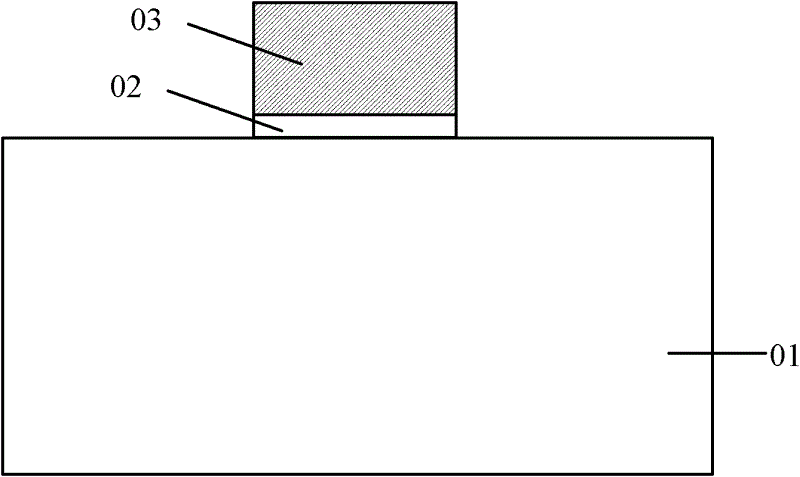
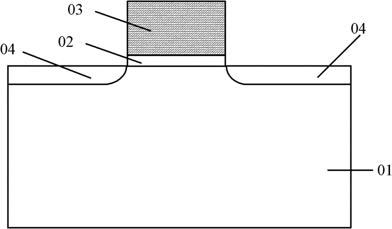
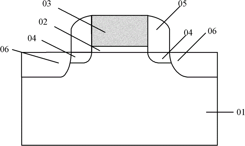
[0048] The short channel effect of the transistor manufactured by the existing method is obvious, and the performance of the device is not ideal. With the development of semiconductor technology, ultra-shallow junction technology is applied to make the source region and the drain region, and the ion lateral diffusion between the source region and the drain region is more serious, which makes the short channel effect more obvious, and the source region and the drain region There is a large junction capacitance and junction leakage current between the drain region and the semiconductor substrate, which reduces the response speed of the device and affects the performance of the device.
[0049] In order to solve the above problems, the inventor proposes a method for manufacturing a transistor, including: providing a semiconductor substrate, a spacer layer is formed on the surface of the semiconductor substrate, and the material of the spacer layer is the same as that of the semico...
PUM
 Abstract
Description
Claims
Application Information
 - R&D Engineer
- R&D Manager
- IP Professional
- Industry Leading Data Capabilities
- Powerful AI technology
- Patent DNA Extraction
Browse by: Latest US Patents, China's latest patents, Technical Efficacy Thesaurus, Application Domain, Technology Topic.
© 2024 PatSnap. All rights reserved.Legal|Privacy policy|Modern Slavery Act Transparency Statement|Sitemap