Dissecting process for diode device

A diode and device technology, applied in the field of anatomy of diode devices, can solve problems such as product chip corrosion, affect the dissection process, change chip shape, etc., to achieve the effects of avoiding damage, ensuring uniform corrosion, and speeding up the response speed

Inactive Publication Date: 2012-08-22
SUZHOU GOODARK ELECTRONICS CO LTD
View PDF2 Cites 12 Cited by
  • Summary
  • Abstract
  • Description
  • Claims
  • Application Information

AI Technical Summary

Problems solved by technology

Both seriously affect the dissection process, and at the same time cause unnecessary corrosion to the product chip, change the shape of the chip, and easily mislead analysts

Method used


Image

  • Dissecting process for diode device
  • Dissecting process for diode device
  • Dissecting process for diode device

Examples


Embodiment

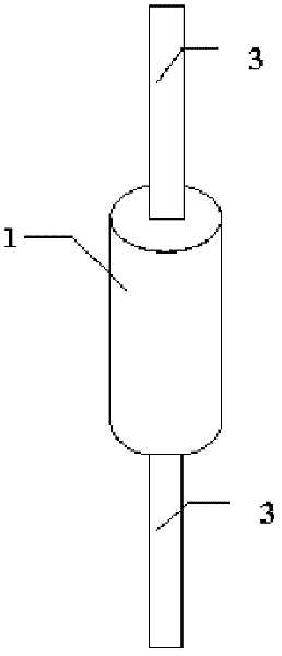
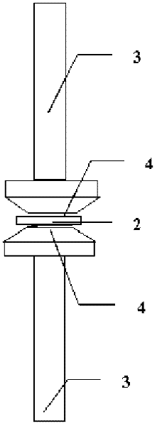
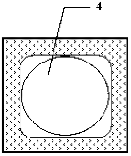
[0025] Embodiment: a kind of dissecting process that is used for diode device, as attached Figure 1-4 As shown, the diode device is composed of a diode chip 2 covered by epoxy resin 1, two copper leads 3 and a solder layer 4 between the surface of the diode chip 2 and the copper leads 3; it is characterized in that: the dissection process Include the following steps:

[0026] Step 1, the concentrated sulfuric acid that concentration in the beaker is 98% is heated to boiling;

[0027] Step 2, place the diode device in the beaker of the step 1, continue to heat, when the diode device exposes the side of the chip and part of the copper lead area, then remove the diode device from the beaker;

[0028] Step 3, place the diode device after step 2 in clear water, and then perform ultrasonic vibration cleaning, and remove the diode device from the clear water after the epoxy resin is removed;

[0029] Step 4. Place the diode device after step 3 in the acetone solution, which can br...


PUM


Abstract

The invention discloses a dissecting process for a diode device. The dissecting process comprises the steps of: 1) continuously heating concentrated sulfuric acid with concentration of 98 percent in a beaker to 95 DEG C; 2) putting the diode device in the concentrated sulfuric acid; 3) putting the diode device in clean water for ultrasonic oscillation cleaning; 4) putting the diode device treated in the step 3 in acetone solution; 5) forming first mixed solution in a beaker by using nitric acid and hydrogen peroxide according to a ratio of 5 to (0.8-1.2) and immersing the diode device in the first mixed solution; 6) forming second mixed solution in a beaker by using nitric acid and water according to a ratio of 5 to (1.8-2.2) and putting the diode device which is decoppered in the step 5) in the second mixed solution in a boiling state and keeping retention time to be 5-10 minutes; and 7) washing the diode device with water, immersing the diode device in acetone solution for oscillation dewatering and keeping washing time to be 20-40 seconds to obtain a diode chip. By adopting the dissecting process, when an epoxy layer is removed, the internal structure of the device is not influenced at all and the reliability of data analysis is greatly improved.

Description

technical field [0001] The invention relates to a method for dissecting electronic components, in particular to a dissecting process for diode devices. Background technique [0002] During the use of electronic components, the product is directly damaged due to the method of use or the design and production defects of the product itself, and the test parameters of the device will also change, resulting in non-compliance with the customer's use standards. How to minimize customer losses and improve product reliability, it is an indispensable job to gradually restore the finished product through technical means and finally find out the source of product failure. Currently, the anatomy method of electronic components mainly adopts The combination of mechanical and chemical methods, using mechanical removal of the epoxy layer around the device, will cause irregular hard strain on the internal structure of the product, which will directly lead to the peeling off of the solder lay...

Claims


Application Information

Patent Timeline
Patent Type & Authority Applications(China)
IPC IPC(8): H01L21/67H01L29/861
Inventor 吴念博滕有西杨生成
Owner SUZHOU GOODARK ELECTRONICS CO LTD
Why Eureka
Try Eureka