Quadruple-junction cascading solar battery and fabrication method thereof
A solar cell and cascading technology, applied in the field of solar cells, can solve the problems of high manufacturing process requirements, complex process, and high cost, and achieve the effects of simple process, reduced growth difficulty, and high yield
- Summary
- Abstract
- Description
- Claims
- Application Information
AI Technical Summary
Problems solved by technology
Method used
Image
Examples
no. 1 Embodiment approach
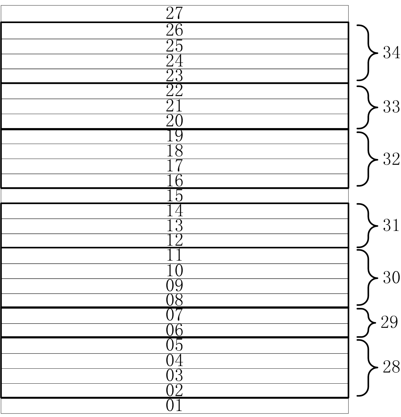
[0027] figure 1 Shown is a schematic structural view of the first specific embodiment of the four-junction cascaded solar cell of the present invention.
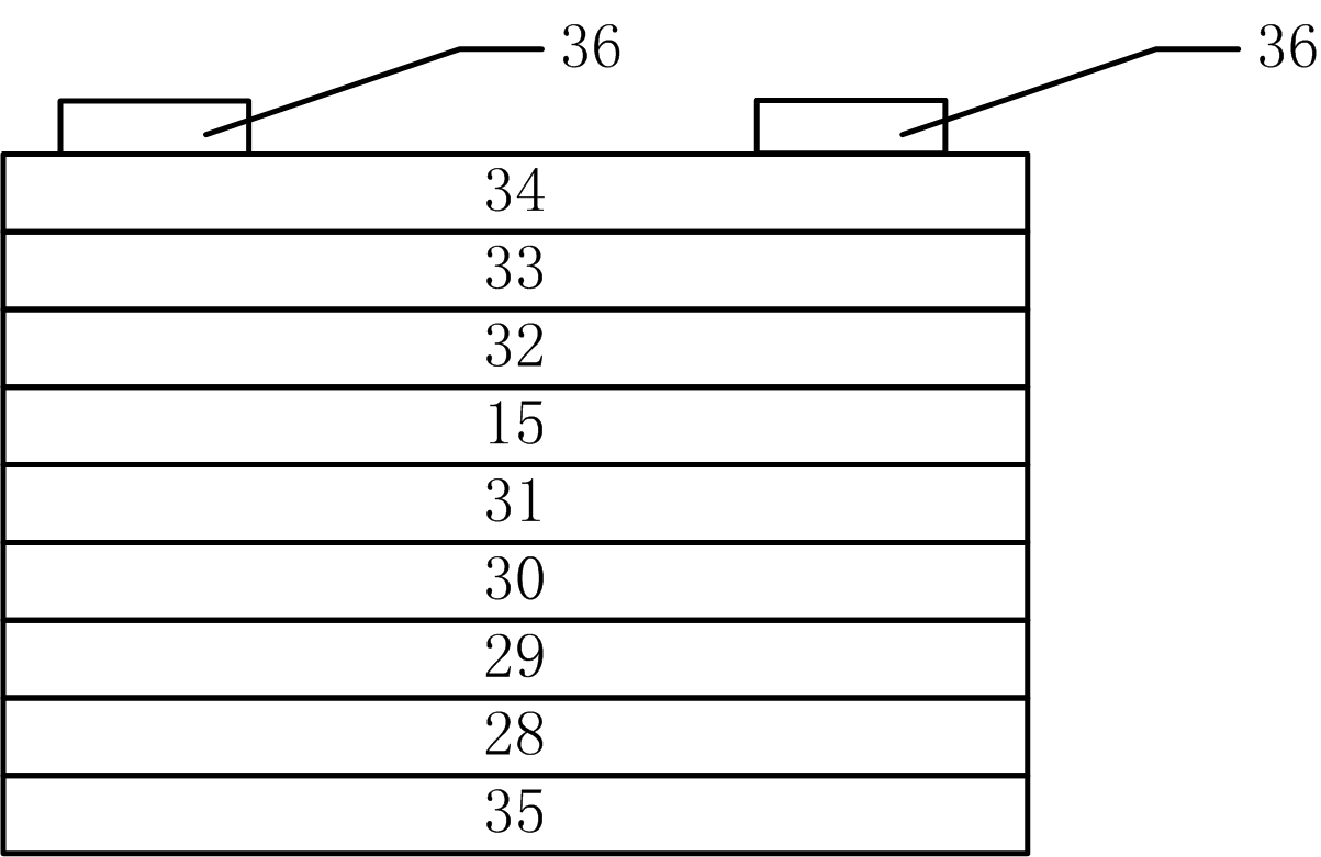
[0028] This embodiment provides a GaInP / GaAs / InGaAsP / InGaAs four-junction cascaded solar cell grown based on the lattice transformation method, which includes an InP substrate layer 01, and InGaAs sub-cells 28, first Tunnel junction 29 , InGaAsP subcell 30 , second tunnel junction 31 , graded transition layer 15 , GaAs subcell 32 , third tunnel junction 33 , GaInP subcell 34 and GaAs contact layer 27 .
[0029] The four-junction cascaded solar cell uses InP as a substrate, which improves the radiation resistance of the cell.
[0030] The four-junction cascaded solar cell is grown by a formal growth method. The top layer GaInP subcell 34 / GaAs subcell 32 is lattice matched to GaAs, and the bottom layer InGaAsP subcell 30 / InGaAs subcell 28 is lattice matched to InP. Wherein, the band gap combinations of the InGaAs sub-cell 2...
no. 2 Embodiment approach
[0043] This embodiment provides a figure 1 In the preparation method of the four-junction cascaded solar cell, the InGaAs sub-cell 28, the first tunnel junction 29, the InGaAsP sub-cell 30, the second tunnel junction 31, and the gradient transition Layer 15 , GaAs subcell 32 , third tunnel junction 33 and GaInP subcell 34 .
[0044] The above-mentioned method for preparing a four-junction cascaded solar cell further includes the step of: growing a GaAs contact layer 27 on the exposed surface of the GaInP sub-cell 34 .
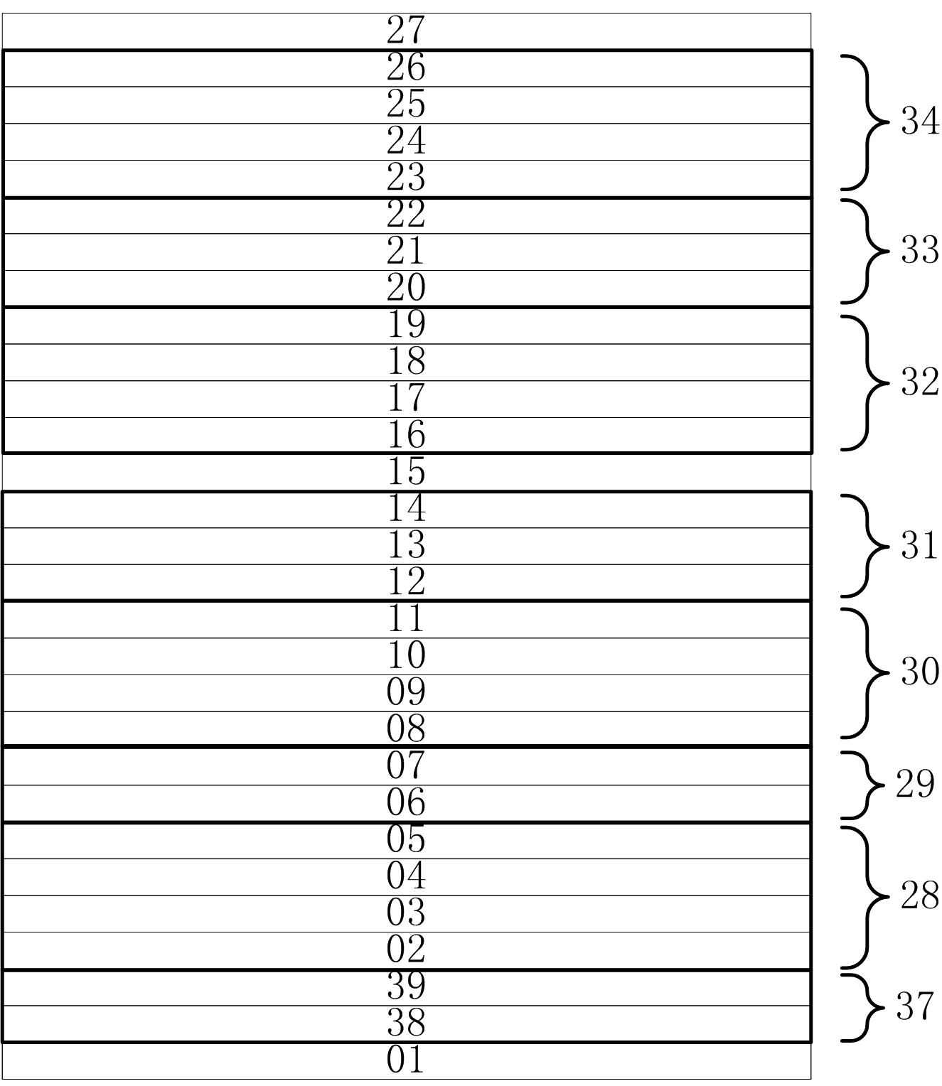
[0045] As an optional implementation, it further includes the step of: growing a fourth tunnel junction between the InP substrate layer 01 and the InGaAs sub-cell 28, the fourth tunnel junction includes N Type doped InGaAs (P) or InP layer and P-type doped InGaAs (P) or InP layer.
[0046] In this embodiment, the preparation method of the four-junction cascaded solar cell further includes the preparation steps of preparing the upper electrode 36 and the lower...
Embodiment 1
[0056] In this embodiment, a method for preparing a GaInP / GaAs / InGaAsP / InGaAs four-junction cascaded solar cell grown by a lattice anomaly growth method based on an InP substrate is provided, comprising the following steps:
[0057] (1) GaInP / GaAs / InGaAsP / InGaAs four-junction cascaded solar cells are grown by MOCVD (Metal Organic Chemical Vapor Deposition, metal organic compound chemical vapor deposition) method, and its structure is as follows figure 1 Shown:
[0058] (1) On the substrate layer 01 of InP with P-type doping, grow with a P-type doping concentration of about 1×10 18 cm -3 The 0.3 micron InP is used as the first back field layer 02 and the P-type doping concentration is about 2×10 17 cm -3 2.5 μm InGaAs is used as the first base region 03 of the InGaAs sub-cell 28, and then grown with an N-type doping concentration of approximately 2×10 18 cm -3 0.2 micron InGaAs is used as the first emitter region 04 of the InGaAs sub-cell 28, regrown with an N-type dopi...
PUM
 Abstract
Description
Claims
Application Information


