Method for etching NiCrSi film through wet process

A technology of wet etching and etching grooves, applied in electrical components, semiconductor/solid-state device manufacturing, circuits, etc., can solve problems such as excessive point defects on the surface of silicon wafers

Active Publication Date: 2014-06-25
NO 24 RES INST OF CETC
View PDF4 Cites 0 Cited by
  • Summary
  • Abstract
  • Description
  • Claims
  • Application Information

AI Technical Summary

Problems solved by technology

[0005] In order to solve the problem that the point defects on the surface of silicon wafers seriously exceed the standard after the existing wet etching NiCrSi film, the present invention proposes a method for wet etching NiCrSi film

Method used


Image

  • Method for etching NiCrSi film through wet process
  • Method for etching NiCrSi film through wet process
  • Method for etching NiCrSi film through wet process

Examples


Embodiment Construction

[0051] In the following, the present invention will be further described in detail in conjunction with the NiCrSi wet etching process implemented in detail.

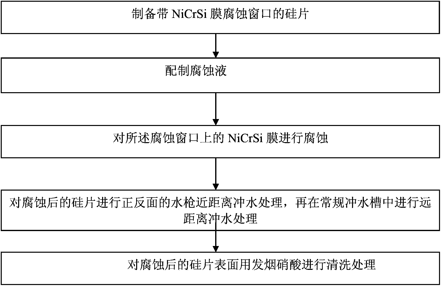
[0052] The technological process of wet etching NiCrSi film of the present invention is as figure 1 shown. The method step of wet etching NiCrSi of the present invention is as follows:

[0053] 1. Prepare a silicon wafer with a NiCrSi film corrosion window.

[0054] 1) Through the process before conventional semiconductor metallization, the product structure before conventional metallization is formed on the single crystal silicon polished wafer;

[0055] 2) Deposit a layer of NiCrSi film with a thickness of 20nm-30nm by using a conventional metallization process;

[0056]3) Carry out the conventional photolithography process, glue coating, exposure, development, and form photoresist as a masking layer, and the NiCrSi film without photoresist as the silicon wafer of the etching window.

[0057] Second, the preparati...


PUM


Abstract

The invention relates to a method for etching a NiCrSi film through a wet process. Since a step of washing the two surfaces of a silicon wafer at a short distance by separately using a water gun, the problem that cerium sulfate on the surface of the silicon wafer is difficult to remove by adopting the existing conventional etching method is effectively solved. Since the product cerium sulfate which is obtained after the NiCrSi film is etched through the wet process is insoluble in water, the method is not suitable for etching multiple silicon wafers which can be etched at one time by adopting the conventional etching method and the method is only suitable for etching the silicon wafers one by one, the cost control of raw materials of the method is superior to the cost control of the raw materials of the conventional etching method. By using fixed supports and culture dishes, the problem that the conventional method is inconvenient to operate is effectively solved; and by using clamping apparatuses which are separately used for placing the silicon wafers and are respectively provided with a lifting handle, the problem of excessive etching of the conventional etching method is effectively solved. After the NiCrSi film is etched by adopting the method, the point defects caused by the cerium sulfate on the surface of the silicon wafer are smaller than 20 per field of view and the qualified rate of the processed surfaces after microscopic examination can reach more than 90%.

Description

technical field [0001] The invention relates to a method for wet etching, in particular to a method for wet etching NiCrSi film, which is suitable for the technical field of semiconductor manufacturing technology. Background technique [0002] Pattern transfer in integrated circuit semiconductor technology means that after forming a photoresist pattern on the surface of a silicon wafer, the pattern is transferred to the layer below the photoresist through an etching process. The wet etch process is a type of etching process in which the silicon wafer is immersed in a chemical solvent that reacts with the exposed film to form soluble by-products. [0003] At present, the common method of wet etching NiCrSi film is to pour the etching solution directly into the etching solution storage tank of the cleaning and etching system according to a certain proportion, put the silicon wafer with the etching window into the PTFE flower basket with a handle, and Put the PTFE flower baske...

Claims


Application Information

Patent Timeline
Patent Type & Authority Patents(China)
IPC IPC(8): H01L21/306H01L21/02
Inventor 王大平梁涛周世远张正元曹阳
Owner NO 24 RES INST OF CETC
Why Eureka
Try Eureka