Power semiconductor module adopting double-sided cooling

A power semiconductor, double-sided cooling technology, applied in the direction of semiconductor devices, semiconductor/solid-state device components, electric solid-state devices, etc., can solve problems such as difficult double-sided cooling, and no substrate design scheme for double-sided cooling, etc. Achieve the effects of improving reliability, excellent thermal management ability, and increasing flow capacity

Active Publication Date: 2012-09-12
株洲菲仕绿能科技有限公司
View PDF8 Cites 31 Cited by
  • Summary
  • Abstract
  • Description
  • Claims
  • Application Information

AI Technical Summary

Problems solved by technology

However, the control terminal of the commonly used IGBT or MOSFET chip is often located in the center of the chip. It is difficult to achieve effective double-sided cooling for chips with this structure using the traditional double-sided cooling method.
In addition, the patent does not provide a substrate design scheme for double-sided cooling in the form of multi-chip parallel connection

Method used


Image

  • Power semiconductor module adopting double-sided cooling
  • Power semiconductor module adopting double-sided cooling
  • Power semiconductor module adopting double-sided cooling

Examples


Embodiment 1

[0027] The power semiconductor module in the embodiment of the present invention is a circuit structure in the form of a half bridge.

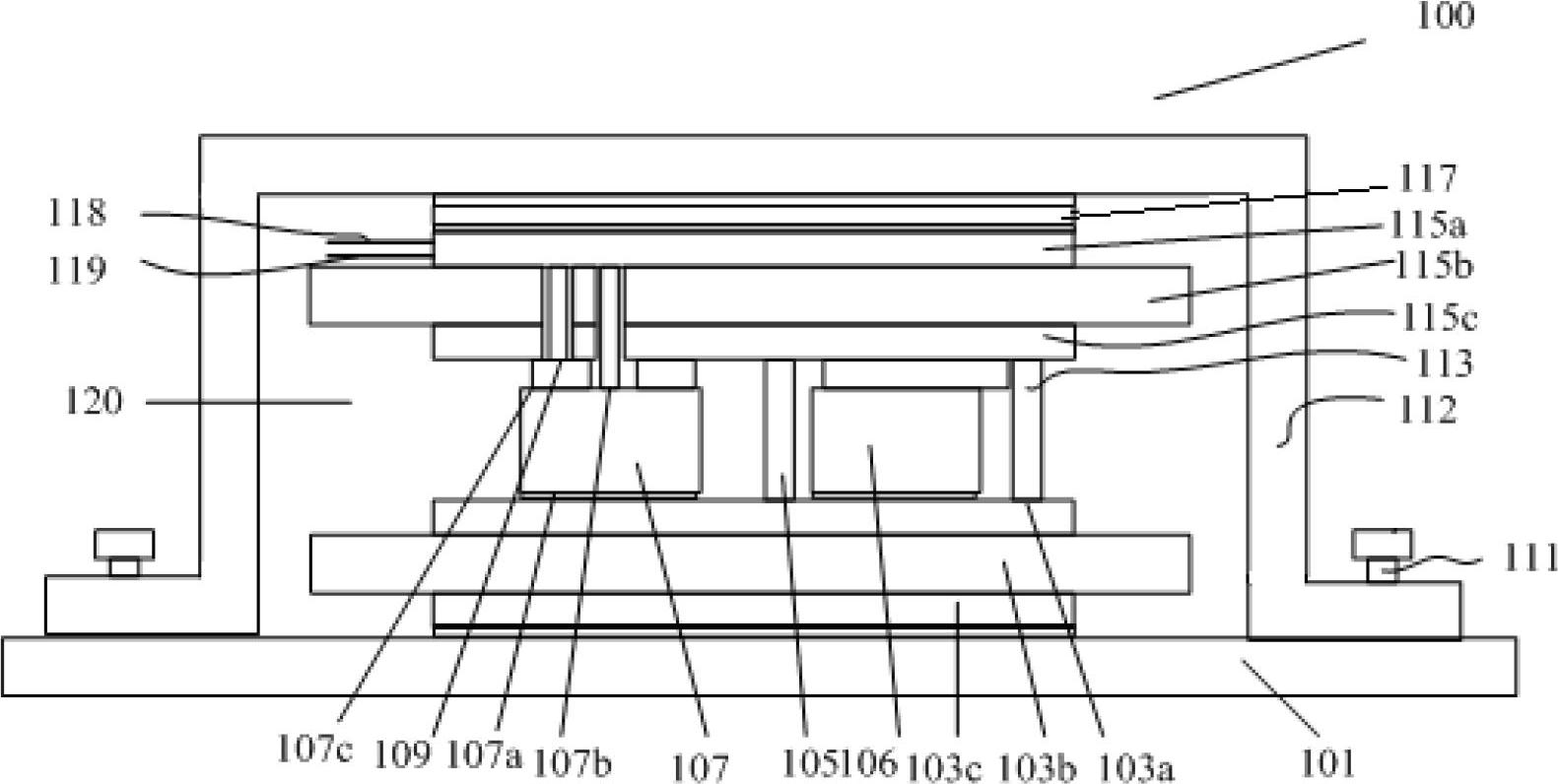
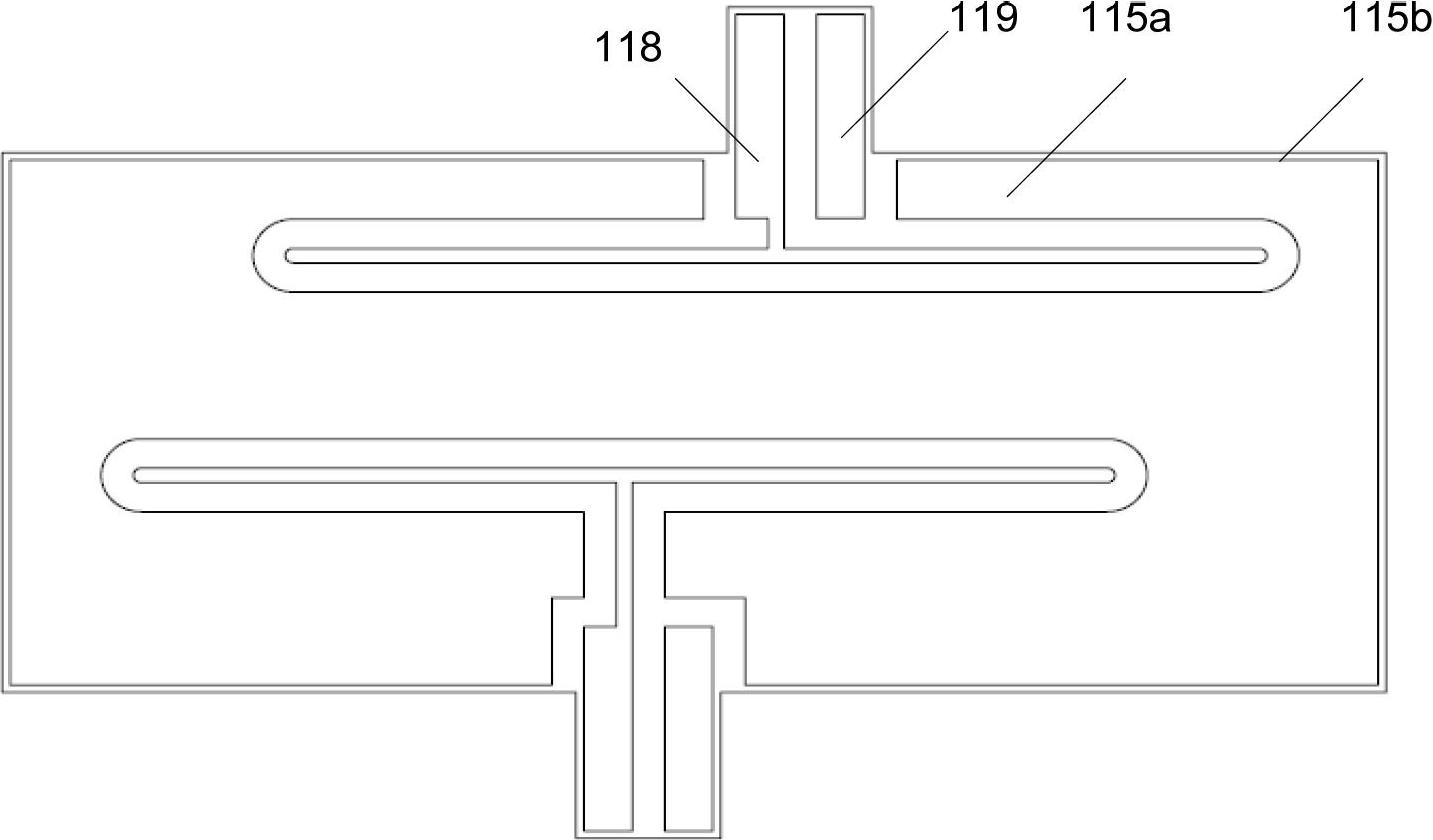
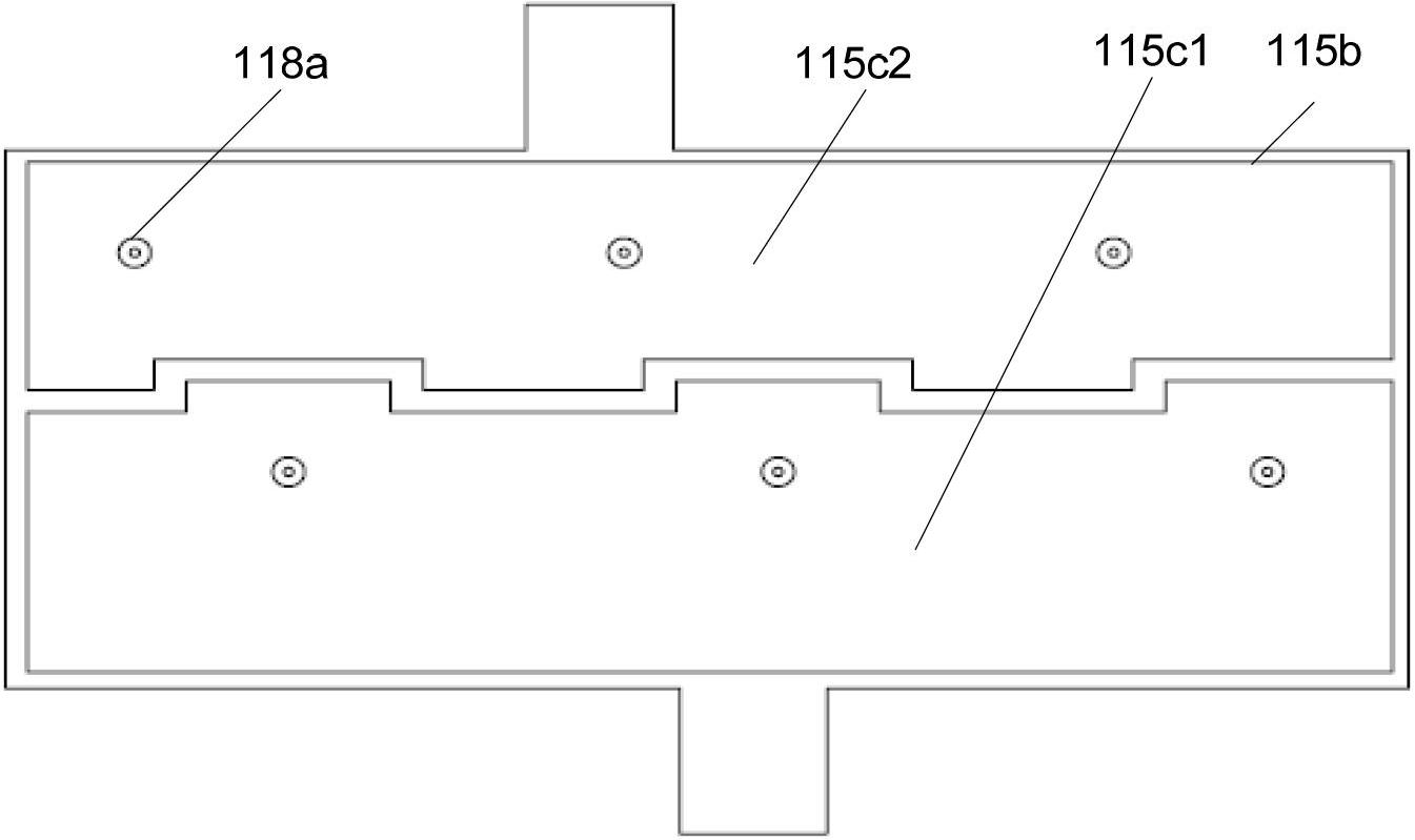
[0028] figure 1 and Figure 7 The power semiconductor module 100 shown is composed of power semiconductor chips 106, 107, substrates 103, 115 cooling plates 101, 112, insulating layer 117, positive terminal 121, negative terminal 123, AC output terminal 122, grid lead-out terminal 118, and The emitter lead-out terminal 119 is formed. The power semiconductor chip includes a fully-controlled power semiconductor chip 107 and an anti-parallel uncontrolled power semiconductor chip 106, and the fully-controlled power semiconductor chip 107 and anti-parallel uncontrolled power semiconductor chip 106 are located in the second between the substrate 103 and the first substrate 115 . Among the two substrates, the first substrate is composed of the first metal layer 115a, the first insulating layer 115b and the second metal layer 115c; the second subst...

Embodiment 2

[0036] Figure 8 to Figure 11 Shown is an embodiment of the second half-bridge structure composed of power semiconductor modules according to the present invention.

[0037] Figure 8 The power semiconductor module 200 shown is composed of power semiconductor chips 205, 206, substrates 203, 215, cooling plates 201, 212, positive terminal 221, negative terminal 223, AC output terminal 222, gate lead-out terminal 218, and emitter lead-out terminal 219 compositions. The power semiconductor chip includes a fully controlled power semiconductor chip 205 and an anti-parallel uncontrolled power semiconductor chip 206 . The full-controlled power semiconductor chip 205 and the anti-parallel uncontrolled power semiconductor chip 206 are located between the first substrate 215 and the second substrate 203 . Among the two substrates, the first substrate is composed of the first metal layer 215a, the first insulating layer 215b and the second metal layer 215c; the second substrate is com...


PUM


Abstract

The invention provides a power semiconductor module adopting double-sided cooling. The power semiconductor module is characterized in that the power semiconductor module (100) contains at least two power semiconductor chips (107, 106) which are arranged between a first substrate (115) and a second substrate (103); each substrate is formed by an intermediate high heat conductivity electric insulation layer and upper and lower metal layers; the metal layers contain circuit structures which realize interconnection between the power semiconductor chips, a positive terminal, a negative terminal, an alternating current output terminal and grid control terminals through welding; the grid control terminals of the power semiconductor chips are arranged in the centers or corners of the chips; a concave cooling plate is reversely installed on an insulation layer (117) or a first metal layer (215a) on the first substrate (115) and the other flat cooling plate is horizontally arranged below the second substrate (103); and the heat of the power semiconductor chips is conducted to the two cooling plates to be dissipated via the first substrate (115) and the second substrate (103), thus realizing double-sided cooling.

Description

technical field [0001] The invention relates to a power semiconductor module. Background technique [0002] With the development of technologies such as hybrid electric vehicles, pure electric vehicles, solar power generation and wind power generation, high-power converters have been widely used. In order to meet the requirements of high power density, the miniaturization of the inverter has become a focus of attention. However, the reduction in size puts forward higher requirements on the heat dissipation and cooling of the power semiconductor module. [0003] At present, high-power semiconductor modules for vehicles generally adopt the method of water circulation single-side cooling and double-side cooling. Patent US2008079021A1 mentions that the junction temperature of power semiconductor chips for vehicles, especially hybrid vehicles, may reach 175°C or even 200°C. Excessively high chip junction temperatures greatly reduce the cycle times of power semiconductor modules...

Claims


Application Information

Patent Timeline
Patent Type & Authority Applications(China)
IPC IPC(8): H01L25/07H01L23/367H01L23/522
CPCH01L2924/0002H01L2924/00
Inventor 钟玉林苏伟孟金磊温旭辉
Owner 株洲菲仕绿能科技有限公司
Why Eureka
Try Eureka