Method for assembling printed circuit board

A technology for a printed circuit board and an assembly method, which is applied in the direction of assembling printed circuits with electrical components, and can solve problems such as low efficiency, complex process, and blisters on the surface of metal substrates.

Active Publication Date: 2012-09-12
COMBA TELECOM SYST CHINA LTD
View PDF3 Cites 9 Cited by
  • Summary
  • Abstract
  • Description
  • Claims
  • Application Information

AI Technical Summary

Problems solved by technology

However, its disadvantages are that the process is complicated and the efficiency is low. High-temperature welding and two-pass fu

Method used


Image

  • Method for assembling printed circuit board
  • Method for assembling printed circuit board
  • Method for assembling printed circuit board

Examples


Embodiment Construction

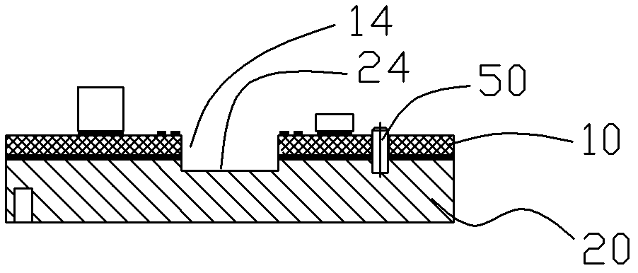
[0020] Aiming at the shortcomings of the prior art, the present invention draws on the high-temperature soldering method and the principle of SMT patch, and provides a new printed circuit board assembly process. The printed circuit board, the power amplifier and the metal substrate are integrated and welded by normal temperature soldering. As a result, the assembly efficiency is improved, the blistering of the metal substrate coating and the deformation of the printed motherboard are avoided, and the ground heat dissipation performance is effectively improved, and the performance of the radio frequency circuit power amplifier is improved.

[0021] The present invention will be further described below in conjunction with the drawings and embodiments.

[0022] See Figure 1-6 According to an embodiment of the present invention, a printed circuit board assembly method includes the following steps:

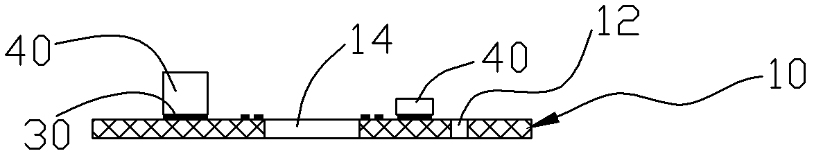
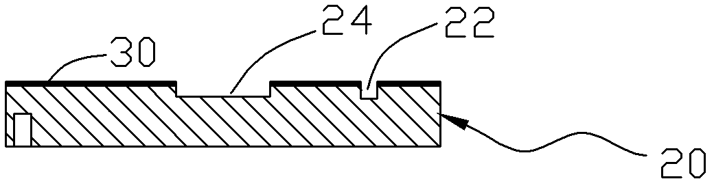
[0023] First, the printed mother board 10 and the metal substrate 20 are provided. The ...


PUM


Abstract

A method for assembling a printed circuit board comprises the steps of providing a printing mother board and a metal substrate, wherein a window is arranged on the printing mother board, components are attached to the printing mother board through a surface mount technology (SMT), and an installation pit which corresponds to the window is arranged on the metal substrate; brushing a uniform layer of normal-temperature soldering tin on an upper surface of the metal substrate, aligning the printing mother board to the metal substrate, enabling the printing mother board and the metal substrate to compress each other tightly, and aligning the window to the installation pit; providing a power amplifier which penetrates through the window and is placed in the installation pit, laying the normal-temperature soldering tin on the contact portion between the power amplifier and the printing mother board and on the contact portion between the power amplifier and the installation pit, and then compressing the power amplifier, the printing mother board and the metal substrate tightly; maintaining the tight compression states between the printing mother board and the metal substrate, between the power amplifier and the printing mother board and between the power amplifier and the metal substrate, and then compressing oppositely to form an assembly to be heated, so that the normal-temperature soldering tin is melted; and cooling down the assembly, so that the printed circuit board is formed.

Description

【Technical Field】 [0001] The invention relates to the technical field of printed circuit board assembly, in particular to a method for assembling a printed mother board and a metal substrate. 【Background technique】 [0002] In order to meet the grounding and heat dissipation requirements of high-power printed circuit boards, a metal substrate with a certain thickness is usually fixed on the bottom of the printed circuit board to ensure that the circuit board itself, on-board components, and high-power components can be rated safely Work at temperature. [0003] At the same time, in order to meet the heat dissipation requirements of high-power components, windows are usually provided for high-power components on the printed circuit board. In this case, the high-power components can be soldered directly through the window or bonded to the metal substrate with conductive and thermal adhesive. This structure has the advantage of good heat dissipation. At the same time, it also provide...

Claims


Application Information

Patent Timeline
IPC IPC(8): H05K3/34
Inventor 杨小平王晓忠梁建长叶维增
Owner COMBA TELECOM SYST CHINA LTD
Why Eureka
Try Eureka