Heating cooling test method and heating cooling test device

A cooling test and cooling device technology, applied in measuring devices, material thermal analysis, instruments, etc., can solve problems such as temperature changes, difficulty in shortening product development time, and greater influence of heating of electronic components, and achieve the effect of simple temperature rise

Inactive Publication Date: 2012-09-19
PANASONIC INTELLECTUAL PROPERTY MANAGEMENT CO LTD
View PDF5 Cites 2 Cited by
  • Summary
  • Abstract
  • Description
  • Claims
  • Application Information

AI Technical Summary

Problems solved by technology

[0004] However, in the above-mentioned existing reliability test, due to the low temperature measurement and high temperature side, in most cases, the time after adding the heating time to the set temperature and the holding time at the set temperature is respectively set as 30 minutes, and more than 1,000 cycles are performed in many cases as the test period, so it takes a long period of about 3 months or more until the test results are obtained, and there is a problem that it is difficult to shorten the product development time
[0005] In addition, in the existing reliability test, since the circuit board mounted with electronic components is placed in its atmosphere, the temperature of the entire circuit board changes, but in the actual use state, the heat generation of a single electronic component The resulting influence is large, resulting in local temperature changes, so there is a problem that the test is performed under conditions that are inconsistent with the actual use environment

Method used


Image

  • Heating cooling test method and heating cooling test device
  • Heating cooling test method and heating cooling test device
  • Heating cooling test method and heating cooling test device

Examples


Embodiment approach 1

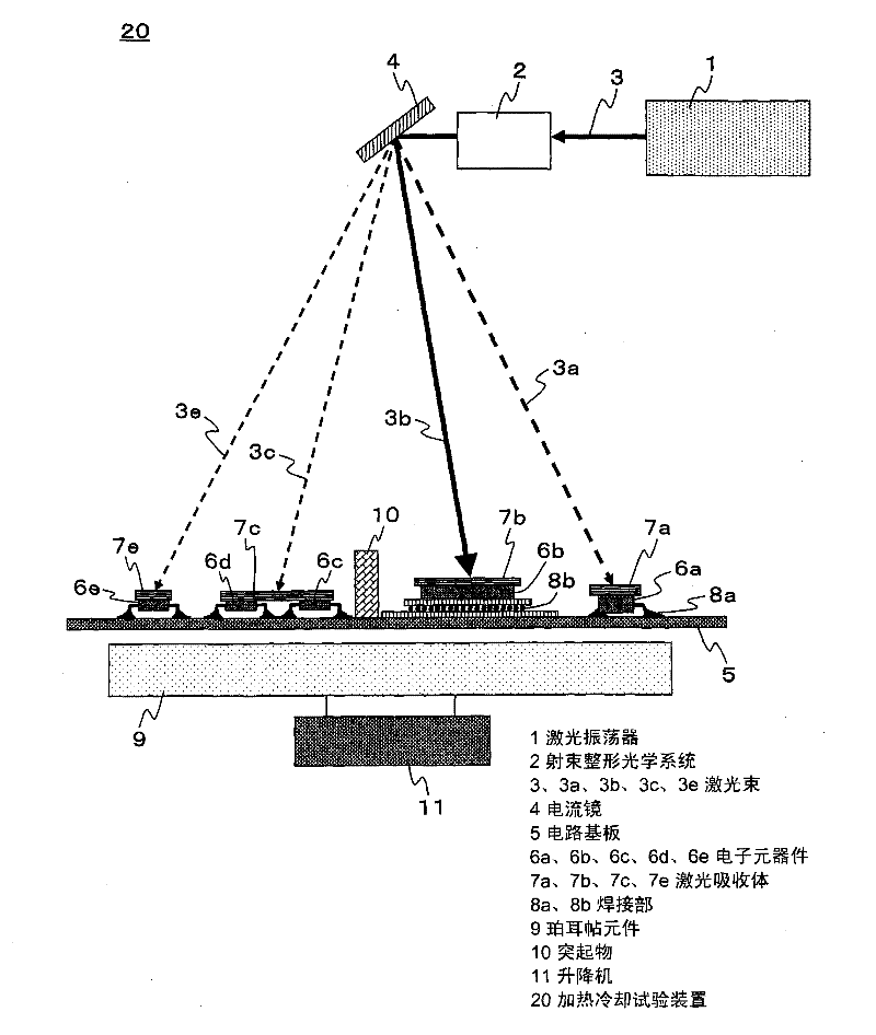
[0104] figure 1 A configuration diagram showing a heating-cooling test device used when implementing the heating-cooling test method in Embodiment 1 of the present invention.

[0105] The outline of the heating and cooling test apparatus 20 according to Embodiment 1 is that laser absorbers 7a, 7b, and 7c are mounted on the upper surfaces of the electronic components 6a to 6e on the circuit board 5 on which a plurality of electronic components 6a to 6e are mounted. , 7e, the laser beam 3 emitted from the laser oscillator 1 is reshaped by the beam shaping optical system 2, and irradiated onto the laser absorbers 7a, 7b, 7c, 7e to make it heated, passing through the laser beam from the laser absorber 7a, The heat conduction of 7b, 7c, and 7e makes the electronic components 6a~6e heat up, after that, the irradiation of the laser beam 3 is stopped, and the solid cooling body (Peltier element 9) is heated from the opposite side where the electronic components 6a~6e are mounted. Th...

Embodiment approach 2

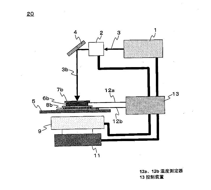
[0156] Figure 9 It is a cross-sectional configuration diagram of a main part of a heating-cooling test device according to Embodiment 2 of the present invention. and figure 2 The same reference numerals are used for the same structural parts.

[0157] Figure 9 It shows the laser irradiation position of the laser beam 3b with respect to the laser absorber 7b on the electronic component 6b.

[0158] In Embodiment 1, such as figure 2 As shown, the laser beam 3b is irradiated so that the optical axis is located substantially in the center of the laser absorber 7b on the electronic component 6b.

[0159] However, in the electronic component 6b constituted by a certain BGA semiconductor package, the IC chip as the heat source 14 may be arranged at a position deviated from the center on the layout inside the electronic component 6b. For the laser absorber 7b in such an electronic component 6b, if the laser beam 3b is irradiated so that the optical axis is located directly ab...

Embodiment approach 3

[0162] Figure 10 It is a block diagram of the heating-cooling test apparatus 21 in Embodiment 3 of this invention at the time of heating. and figure 2 The same reference numerals are used for the same structural parts.

[0163] like Figure 10 As shown, the control device 13 of the third embodiment controls the galvano mirror 4 so that the laser beam 3b scans the entire surface of the laser absorber 7b on the electronic component 6b.

[0164] In the structures of Embodiments 1 and 2, the laser beam 3b is fixed to irradiate the predetermined position of the laser absorber 7b on the electronic component 6b, so the area of ​​the electronic component 6b is relatively smaller than the laser beam diameter of the irradiated laser beam 3b. If it is too large, it may not be possible to completely and uniformly heat the entire surface of the laser absorber 7b.

[0165] For example, when the electronic component 6b is 30mm square and the laser absorber 7b is 35mm square, when the l...


PUM


Abstract

The invention provides a heating cooling test method and a heating cooling test device which can simply heat in a heating up process without Peltier 's elements. The heating cooling test method is used for evaluating circuit board which is equipped with electronic components (6a-6e) and comprises the steps of heating up the electronic components, cooling the electronic components and alternatively heating up and cooling the electronic components, wherein in the step of heating, laser absorbers (7a,7b,7c,7e) equipped on the electronic components irradiate laser beams (3a,3b,3c,3e) for heating to heat the electronic components.

Description

technical field [0001] The present invention relates to a connection reliability test after electronic components are mounted on a circuit board, and particularly relates to a heating-cooling test method and a heating-cooling test device for a connection reliability test in a soldered portion. Background technique [0002] As a conventional heating and cooling test method, the following method is used: a test sample with electronic components mounted on a circuit board is placed in a large constant temperature furnace, and the holding time of low temperature and high temperature is specified as the test condition, and repeated temperature is applied. After that, when the specified cycle is over, take out the test sample, and estimate the life of the connection reliability by checking the conduction resistance, solder joint strength, and metal structure changes of the soldered part during the temperature cycle. Also in the case of measuring the conduction resistance, a method...

Claims


Application Information

Patent Timeline
IPC IPC(8): G01N3/60G01N25/00
CPCG01R31/2806G01R31/2817
Inventor 船见浩司小野之良金岛敬之介
Owner PANASONIC INTELLECTUAL PROPERTY MANAGEMENT CO LTD
Why Eureka
Try Eureka