Complementary metal oxide semiconductor (CMOS) image sensor and manufacturing method thereof

A technology of image sensor and manufacturing method, which is applied in radiation control devices and other directions, can solve problems such as crosstalk of CMOS image sensors, and achieve the effect of avoiding crosstalk

Inactive Publication Date: 2012-09-19
BRIGATES MICROELECTRONICS KUNSHAN
View PDF6 Cites 6 Cited by
  • Summary
  • Abstract
  • Description
  • Claims
  • Application Information

AI Technical Summary

Problems solved by technology

[0006] The problem solved by the present invention is to propose a new CMOS image sensor...

Method used


Image

  • Complementary metal oxide semiconductor (CMOS) image sensor and manufacturing method thereof
  • Complementary metal oxide semiconductor (CMOS) image sensor and manufacturing method thereof
  • Complementary metal oxide semiconductor (CMOS) image sensor and manufacturing method thereof

Examples


Embodiment 1

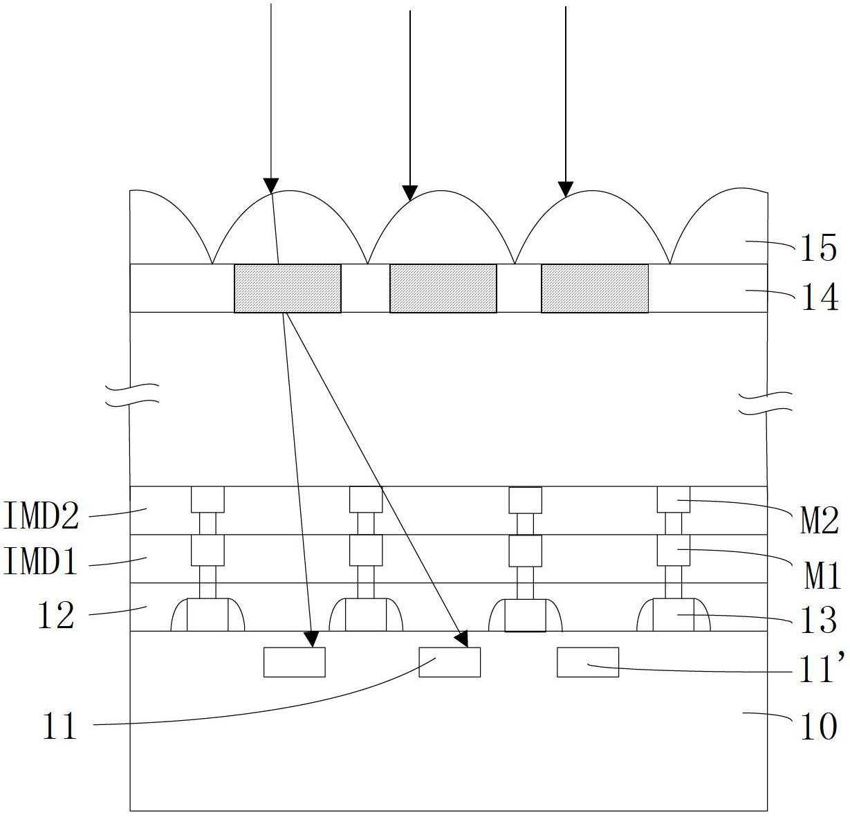
[0044] The following combination figure 2 The CMOS image sensor shown and image 3 The flow chart of the manufacturing method of the image sensor is shown, and the CMOS image sensor provided in the first embodiment and the mechanism for solving the crosstalk problem are introduced in detail.

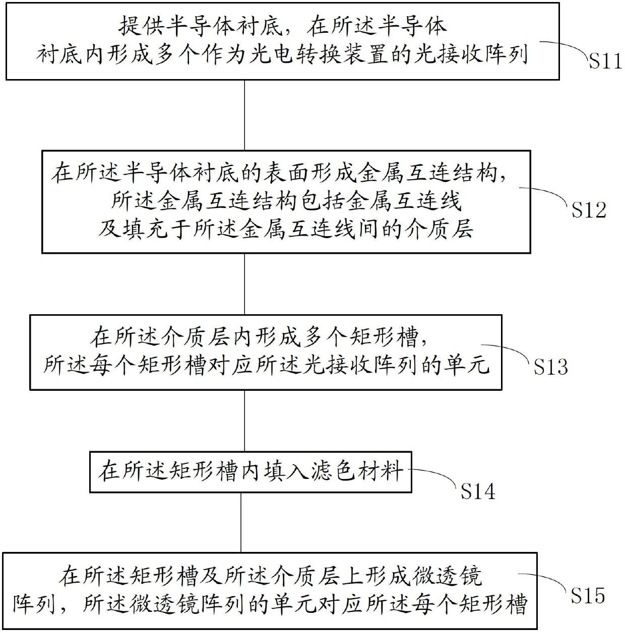
[0045] First introduce the production method. combine image 3 and figure 2 As shown, step S11 is executed to provide a semiconductor substrate 20 in which a light-receiving array serving as a photoelectric conversion device is formed.

[0046] The material of the semiconductor substrate 20 in this embodiment may be silicon, germanium, silicon-germanium, etc., but is not limited to the above materials. The light-receiving array is an array formed by existing photosensitive elements as units, for example, more photodiodes 21, 21' are used, and its core structure is a PN junction. Compared with ordinary diodes, the difference in structure is: in order to receive When the incident li...

Embodiment 2

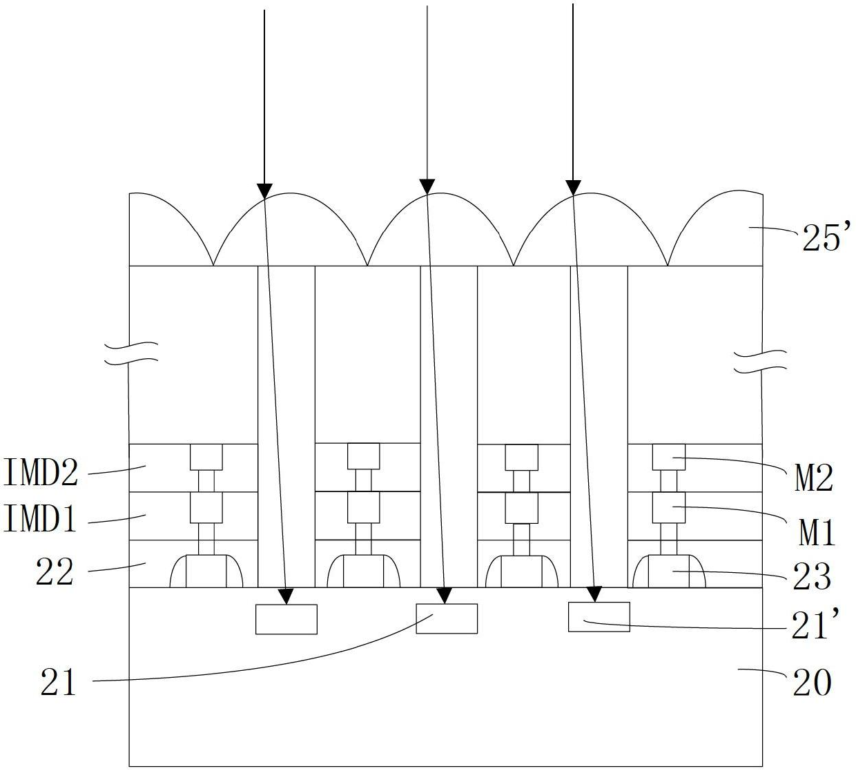
[0063] It can be seen that, in the first embodiment, since the shape of the groove is rectangular, the units of the color filter array are also rectangular. The inventor found in practice that adopting a groove with a small wedge-shaped structure at the bottom, such as Figure 8 As shown in , compared with the rectangular color filter unit, the formed color filter unit has a better capability of restricting the light propagating therein, thus improving the crosstalk effect better.

[0064] Correspondingly, the manufacturing method of the CMOS image sensor in this step is roughly the same as that in the first embodiment. The difference is that the new step S13' is: forming a plurality of wedge-shaped grooves in the dielectric layer, and the smaller bottom of each wedge-shaped groove corresponds to each unit of the light-receiving array.

[0065] The area of ​​the dielectric layer in this step is the same as that in the first embodiment, and there are many ways to form the wedg...

Embodiment 3

[0067] In the CMOS image sensor of the third embodiment, on the basis of the CMOS image sensors provided in the first and second embodiments, a reflective layer is added on the side wall of the groove, so as to further limit the propagation of light in the color filter unit. Taking the wedge-shaped groove as an example, the cross-sectional schematic diagram of the CMOS image sensor including the reflective layer 26 is as follows: Figure 9 shown.

[0068] Specifically, the side wall of the reflective layer is made of aluminum, and may also be made of other materials that can realize the reflective function.

[0069] Correspondingly, the manufacturing method of the CMOS image sensor in this step is roughly the same as that in the first embodiment. The difference is that the new step S13" is: forming a plurality of rectangular or wedge-shaped grooves in the dielectric layer, and when the grooves are wedge-shaped, the smaller bottom of each wedge-shaped corresponding to each of ...


PUM


Abstract

The invention discloses a complementary metal oxide semiconductor (CMOS) image sensor, which comprises an optical receiving array, a metal interconnection structure, a color filter array and a micro-lens array, wherein the optical receiving array serves as a photoelectric conversion device; the metal interconnection structure is arranged on the optical receiving array and comprises metal interconnection lines and a medium layer which is filled between the metal interconnection lines; the color filter array is arranged on the optical receiving array; the micro-lens array is arranged on the metal interconnection structure; the optical receiving array, the color filter array and the micro-lens array respectively comprise a plurality of units; the units of the color filter array are positioned in the medium layer of the metal interconnection structure and separated by the metal interconnection lines of the metal interconnection structure; and the units of the color filter array, the units of the optical receiving array and the units of the micro-lens array are respectively opposite to one another. Moreover, the invention also provides a manufacturing method of the CMOS image sensor. By adoption of the technical scheme provided by the invention, the problem of crosstalk of the CMOS image sensor can be solved.

Description

technical field [0001] The invention relates to the field of semiconductor manufacturing, in particular to a CMOS image sensor and a manufacturing method thereof. Background technique [0002] Image sensors currently entering the market are divided into complementary metal oxide semiconductor (Complementary Metal Oxide Semiconductor, CMOS) sensors and charge-coupled device (Charge-coupled Device, CCD) sensors. CMOS or CCD sensors usually have hundreds of thousands or even millions of pixels to convert light signals into electrical signals, so that the original images of people or objects are converted into electrical signals in the image sensor. CMOS or CCD image sensors have been widely used in various digital image devices, such as digital cameras, digital video cameras and other electronic devices, due to their advantages of small size, low power consumption, and low cost. [0003] Regarding the structure of the CMOS image sensor in the prior art, such as figure 1 As sh...

Claims


Application Information

Patent Timeline
IPC IPC(8): H01L27/146
Inventor 陈雷
Owner BRIGATES MICROELECTRONICS KUNSHAN
Why Eureka
Try Eureka