Novel low end metal oxide semiconductor field effect transistor (MOSFET)/ insulated gate bipolar transistor (IGBT) negative pressure clamping driving circuit and control method thereof

A technology of drive circuit and control method, which is applied in the direction of electrical components, output power conversion devices, etc., can solve problems such as increased switching loss, achieve the effects of preventing false conduction, accelerating switching speed, and improving anti-interference ability

Active Publication Date: 2014-06-18
马鞍山市安工大智能装备技术研究院有限公司
View PDF4 Cites 0 Cited by
  • Summary
  • Abstract
  • Description
  • Claims
  • Application Information

AI Technical Summary

Problems solved by technology

[0005] A low-end MOSFET negative pressure clamping drive circuit and its control method are proposed to solve the problems in the prior art that the switching loss is increased due to the continuous increase of the switching frequency. The circuit and method of the present invention accelerate the switching tube The switching speed improves the anti-interference ability of the drive circuit, which can effectively prevent the false conduction of the switching device

Method used


Image

  • Novel low end metal oxide semiconductor field effect transistor (MOSFET)/ insulated gate bipolar transistor (IGBT) negative pressure clamping driving circuit and control method thereof
  • Novel low end metal oxide semiconductor field effect transistor (MOSFET)/ insulated gate bipolar transistor (IGBT) negative pressure clamping driving circuit and control method thereof
  • Novel low end metal oxide semiconductor field effect transistor (MOSFET)/ insulated gate bipolar transistor (IGBT) negative pressure clamping driving circuit and control method thereof

Examples


Embodiment 1

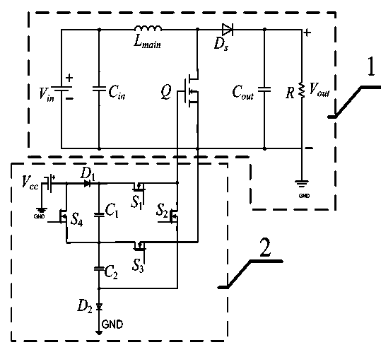
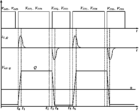
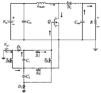
[0043] Such as figure 1 , the low-side MOSFET negative voltage clamp driving circuit of the present embodiment, which includes a BOOST step-up unit 1 and a negative voltage driving clamp unit 2 . figure 2 It is a waveform diagram of relevant parameters of the low-side MOSFET negative voltage clamp drive circuit. It can be seen from the figure that within one cycle, that is, from t 0 -t 6 During this period of time, the working modes of the switching tube Q can be divided into 6, and each working mode is as follows: Figure 3 ~ Figure 8 shown.

[0044] BOOST step-up unit 1 is powered by 14V input power V in , 50uf input capacitor C in , 50uH inductance L main , MOSFET switch tube Q and diode D of model FQDN10TM S , 10uF output capacitor C out Composed with a 20Ω load resistor R, the input power supply V in with input capacitance C in in parallel, the inductance L main , Diode D S and output capacitor C out in series with the input capacitor C in in parallel, the ...


PUM


Abstract

The invention discloses a novel low end metal oxide semiconductor field effect transistor (MOSFET) / insulated gate bipolar transistor (IGBT) negative pressure clamping driving circuit and a control method thereof which belong to the field of power electronic driving. The driving circuit comprises a negative pressure clamping driving unit and a BOOST unit which are in circuit connection. The control method includes the following steps: (1) controlling S1 and S4 to be in connection state and S2 and S3 to be in disconnection state; (2) controlling the S1, the S2, the S3 and the S4 to be in the disconnection state and maintaining voltage on a Q gate source electrode at U3; (3) controlling the S2 and the S3 to be in the connection state and the S1 and the S4 to be in the disconnection state, enabling voltage on the Q gate source electrode to be clamped on the voltage U4 and enabling the Q to be disconnected instantaneously; and (4) controlling the S1, the S2, the S3 and the S4 to be in the connection state and maintaining voltage on the Q gate source electrode at U4. The S1, the S2, the S3 and the S4 stand for different MOSFET switch tubes. The driving circuit and the control method improve anti-jamming capability and can effectively prevent error connection of switch devices.

Description

technical field [0001] The invention belongs to the field of power electronic driving, and more specifically relates to a driving circuit for negative pressure driving a switching tube and a circuit control method thereof. Background technique [0002] In recent years, with the development of technology, the switching frequency driven by the voltage source has gradually exceeded 1MHz, but the switching frequency is too high, which will bring a series of problems, among which the main obstacle hindering the increase of the switching frequency driven by the voltage source is the switching device The loss in the turn-on and turn-off process, the loss of the gate drive and the loss of the output capacitance of the switching device, and the current source drive can just solve the above problems, it can greatly increase the switching frequency of the switching tube and reduce the switching loss, so is widely used. [0003] The current source drive charges and discharges the switc...

Claims


Application Information

Patent Timeline
Patent Type & Authority Patents(China)
IPC IPC(8): H02M1/088
Inventor 陈宗祥葛芦生何胜方宋斌
Owner 马鞍山市安工大智能装备技术研究院有限公司
Why Eureka
Try Eureka