A method for improving the turn-off performance of an insulated gate bipolar transistor
A bipolar transistor and insulated gate technology, applied in semiconductor devices, electrical components, circuits, etc., can solve the problems of slow hole extraction speed, small turn-off energy loss, high turn-off energy loss, etc., to improve turn-off loss , low turn-off loss, and improved conduction voltage drop
- Summary
- Abstract
- Description
- Claims
- Application Information
AI Technical Summary
Problems solved by technology
Method used
Image
Examples
Embodiment 1
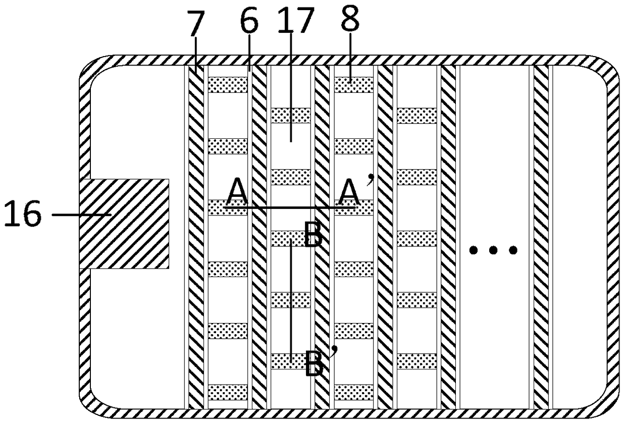
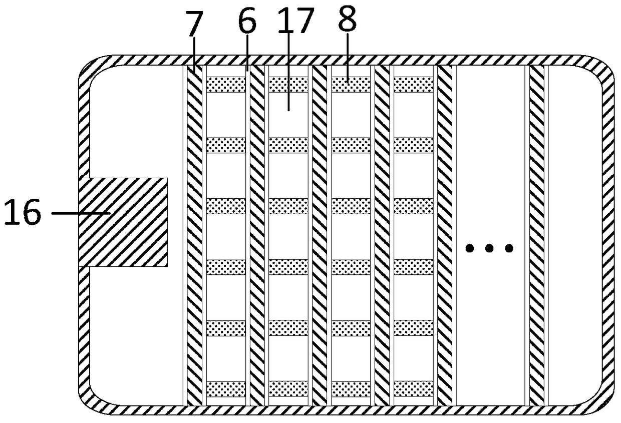
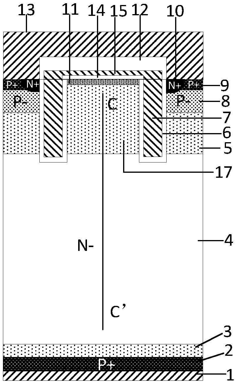
[0029] An insulated gate bipolar transistor comprising: a heavily doped P-type collector region 2, a collector metal 1 is provided on the back of the heavily doped P-type collector region 2, and a lightly doped N-type buffer is provided on the front side Layer 3, the lightly doped N-type buffer layer 3 is provided with a lightly doped N-type base region 4, and the lightly doped N-type base region 4 is provided with a lightly doped N-type carrier storage layer 5. The doped N-type carrier storage layer 5 is provided with trench gates parallel to each other. The trench gates are composed of a first type gate oxide layer 6 and a first polysilicon gate 7. The layer 6 is located between the first polysilicon gate 7 and the lightly doped N-type carrier storage layer 5. The trench gate has a deep depth into the lightly doped N-type base region 4, and the trench gate is lightly doped with N Type carrier storage layer 5 is divided into strips, the strip lightly doped N-type carrier stora...
Embodiment 2
[0036] A method for manufacturing an insulated gate bipolar transistor with improved turn-off performance includes:
[0037] Step 1: First select N-type silicon material as the substrate and epitaxially grow a shallow doped N-type epitaxial layer;
[0038] The second step: ion implantation of N-type impurities and annealing to form lightly doped N-type carrier storage layer 5;
[0039] The third step: etching the trench, and forming the first type gate oxide layer 6 and the second type gate oxide layer 14;
[0040] The fourth step: deposit polysilicon, and etch to form the first polysilicon gate 7;
[0041] The fifth step: selective ion implantation of P-type impurities, and annealing to form a lightly doped P-type body region 8;
[0042] The sixth step: ion implantation of P-type impurities, and annealing to form a lightly doped shallow P well 11;
[0043] The seventh step: deposit polysilicon to form a second polysilicon gate 15;
[0044] Step 8: Selectively etch the light second polysil...
PUM
 Abstract
Description
Claims
Application Information


