Supercharge Your Innovation With Domain-Expert AI Agents!

Optical sensing system based on planar optical waveguide

A planar optical waveguide and optical sensing technology, applied in the field of optical sensing, to achieve the effects of easy processing, simple structure, and easy mass production

Active Publication Date: 2015-06-03
KUANG CHI INST OF ADVANCED TECH +1
View PDF5 Cites 0 Cited by
  • Summary
  • Abstract
  • Description
  • Claims
  • Application Information

AI Technical Summary

Problems solved by technology

However, since there have been no major breakthroughs in structural design and production technology, this type of sensor has been limited by the size and materials of optical devices. etching or nanoimprint technology) and it is difficult to simultaneously integrate complex optoelectronic properties on a single chip

Method used


Image

  • Optical sensing system based on planar optical waveguide
  • Optical sensing system based on planar optical waveguide
  • Optical sensing system based on planar optical waveguide

Examples


Embodiment Construction

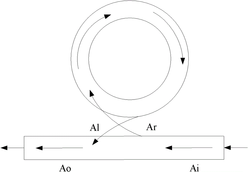
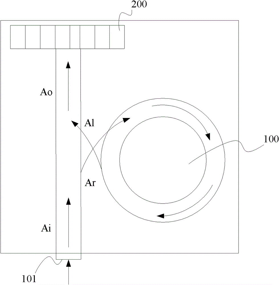
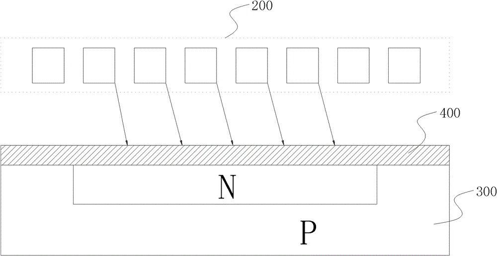
[0018] The invention provides an optical sensing system based on a planar optical waveguide, which includes an optical sensor integrated on a CMOS chip and an arithmetic circuit connected with the optical sensor. The optical sensor is formed by an array of sensing units, and the sensing unit includes The planar optical waveguide 100, the coupling grating 200 and the PN junction 300, the coupling grating 200 couples the optical signal output by the planar optical waveguide to the PN junction 300, the PN junction 300 is connected to the operation circuit, and the operation circuit performs the signal output from the PN junction 300 Calculate the result to be measured.

[0019] The present invention will be described in detail below taking the microring resonator as a planar optical waveguide as an example. figure 2 : The input optical signal is coupled into the microring resonator through the single-mode fiber 101; then, in the coupling region of the waveguide structure, a part...


PUM


Abstract

The invention provides an optical sensing system based on a planar optical waveguide. The system comprises an optical sensor integratedly arranged on a CMOS chip and an operation circuit connected with the optical sensor. The optical sensor is formed by a sensing unit array. The sensing unit comprises the planar optical waveguide, a coupling grating and a PN junction. The coupling grating couples an optical signal output by the planar optical waveguide to the PN junction. The PN junction is connected with the operation circuit. The system of the invention has the following advantages that: the planar optical waveguide and the optical sensor are integrated on the same chip through a COMS technology; a structure is simple; the system is processed easily and is suitable for large-scale production.

Description

【Technical field】 [0001] The invention relates to the field of optical sensing, in particular to an optical sensing system based on a planar optical waveguide. 【Background technique】 [0002] At present, as an important branch of information science and technology, optical sensing technology has very important applications in many aspects such as optical communication, industrial process control, environmental monitoring and national security. Optical sensing technology can solve the problems of low sensitivity, susceptibility to interference, long sensing time, and unsafe detection of certain chemical gases in electrical sensing technology; in contrast, optical sensors have high sensitivity, small size, It has many advantages such as strong anti-electromagnetic interference ability, easy integration, and online detection. Therefore, in the field of sensing, light sensing plays an increasingly important role. [0003] In recent years, as a very important member of sensor t...

Claims


Application Information

Patent Timeline
Patent Type & Authority Patents(China)
IPC IPC(8): G01D5/34
Inventor 刘若鹏栾琳赵治亚孙豪文
Owner KUANG CHI INST OF ADVANCED TECH
Features
  • R&D
  • Intellectual Property
  • Life Sciences
  • Materials
  • Tech Scout
  • Unparalleled Data Quality
  • Higher Quality Content
  • 60% Fewer Hallucinations
Learn More