Organic light-emitting diode display panel and manufacturing method thereof

A technology for light-emitting diodes and display panels, which is applied to electroluminescent light sources, photo-engraving processes of patterned surfaces, semiconductor/solid-state device manufacturing, etc. Influence and other problems, to achieve the effect of simplifying the production process, reducing the production cost, and saving the mask alignment process

Active Publication Date: 2012-10-03
BOE TECH GRP CO LTD
View PDF6 Cites 20 Cited by
  • Summary
  • Abstract
  • Description
  • Claims
  • Application Information

AI Technical Summary

Problems solved by technology

[0008] It can be seen that in the prior art, a special mask plate and an alignment process are required when manufacturing the pixel defining layer, so the manufacturing process is relatively complicated and the manufacturing cost is high; and, since an alignment process is required, the display The yield rate of the panel will be affected by the alignment accuracy

Method used


Image

  • Organic light-emitting diode display panel and manufacturing method thereof
  • Organic light-emitting diode display panel and manufacturing method thereof
  • Organic light-emitting diode display panel and manufacturing method thereof

Examples


Embodiment Construction

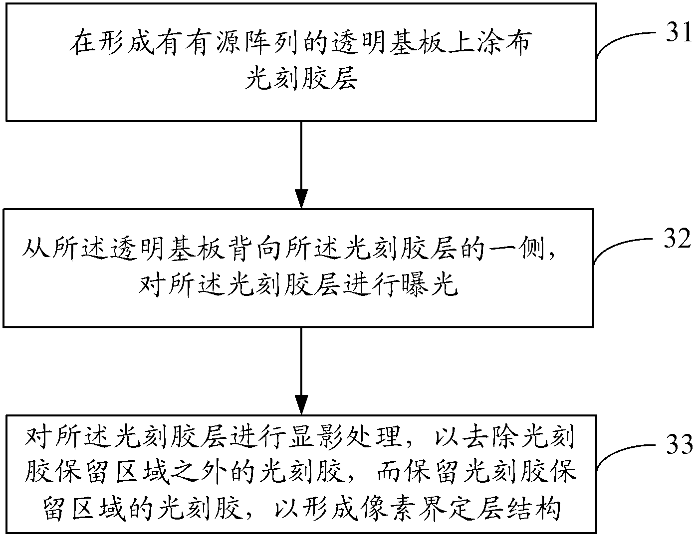
[0044] The method for manufacturing the pixel-defining layer of an OLED display panel provided by the embodiment of the present invention does not require a special mask, and does not require an alignment process during the photolithography process, thereby reducing production costs, simplifying the production process, and Improve product yield. In order to make the object, technical solution and advantages of the present invention clearer, the present invention will be described in detail below with reference to the accompanying drawings and specific embodiments.

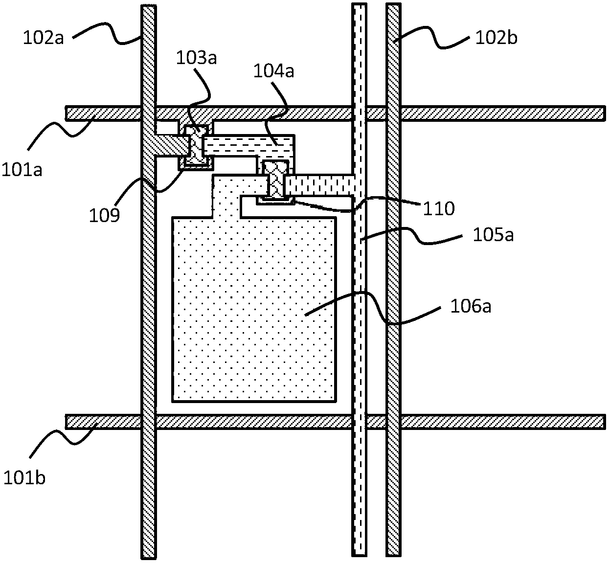
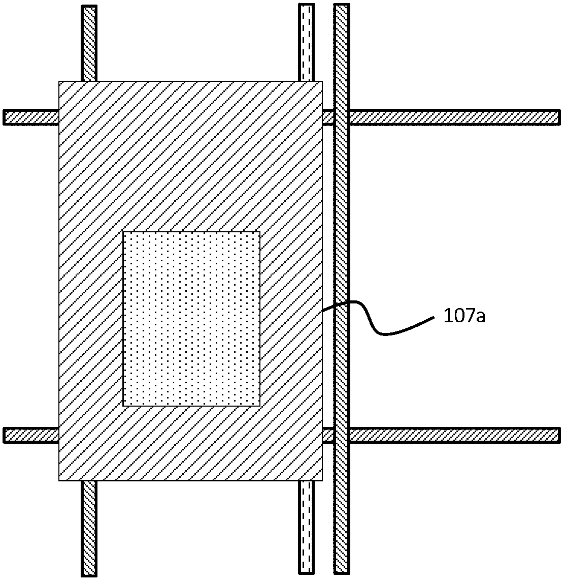
[0045] The pixel defining layer of the OLED display panel in the embodiment of the present invention is prepared after the active array and the anode of the pixel are prepared, and before the formation of the organic light emitting layer.

[0046] The traditional pixel definition layer usually uses a specially designed mask to pattern the pixel definition layer. The embodiment of the present invention does not req...


PUM


Abstract

The invention provides an organic light-emitting diode display panel and a manufacturing method of the organic light-emitting diode display panel, relating to the technical field of display. The manufacturing method comprises the following steps: coating a photoresist layer on a transparent substrate with an active array, wherein the active array comprises a driving power line, a data line and a scanning line, and at least one of the data line and the driving power line and the scanning line are not transparent; exposing the photoresist layer at one side of the transparent substrate, which is opposite to the photoresist layer; exposing the photoresist layer and utilizing the scanning line and at least one line to be used as a mask to prevent corresponding photoresist from being exposed so as to form a photoresist retaining region by the photoresist layer; carrying out developing treatment on the photoresist layer to remove the photoresist outside the photoresist retaining region; and retaining the photoresist in the photoresist retaining region to form an imaging pixel defining layer structure. According to the organic light-emitting diode display panel and the manufacturing method, a manufacturing process of a display panel is simplified, the manufacturing cost of the display panel is reduced and the yield of the display panel is increased.

Description

technical field [0001] The invention relates to the display field, in particular to an organic light emitting diode display panel and a manufacturing method thereof. Background technique [0002] Organic light-emitting diode (OLED, Organic Light-Emitting Diode) display backplane usually consists of glass substrate, ITO (indium tin oxide, indium tin oxide) anode (Anode), organic light-emitting layer (Emitting Material Layer) and cathode (Cathode), etc. The organic light-emitting layer is sandwiched between the thin and transparent ITO anode and the metal cathode. When the holes (Hole) of the anode and the electrons (Electron) from the cathode are combined in the organic light-emitting layer, the The organic material in the organic light-emitting layer is excited to emit light. Active Matrix Organic Light Emitting Diode (AMOLED, Active Matrix / Organic Light Emitting Diode) display panel is a type of OLED display panel. Compared with traditional liquid crystal display panels, A...

Claims


Application Information

Patent Timeline
Patent Type & Authority Applications(China)
IPC IPC(8): H01L21/77H01L27/32H05B44/00
CPCH01L27/32G03F7/00H10K59/122H10K71/00H10K59/00
Inventor 陈海晶
Owner BOE TECH GRP CO LTD
Why Eureka
Try Eureka