
Miniature eddy current sensor with structure consisting of silicon substrate and multilayer coils

An eddy current sensor and multi-layer coil technology, applied in the field of micro-sensors, can solve the problems of increasing preparation time, prolonging the detection period, and large human radiation, so as to increase the area of ​​flaw detection, improve the detection efficiency, and increase the detection area.

Inactive Publication Date: 2012-10-10
DALIAN UNIV OF TECH
View PDF9 Cites 13 Cited by
  • Summary
  • Abstract
  • Description
  • Claims
  • Application Information

AI Technical Summary

Problems solved by technology

[0003] Magnetic particle flaw detectors have certain disadvantages: for example, the detection sensitivity of micro-cracks on the surface is relatively low, and it is difficult to find defects; it is necessary to pre-treat the surface of the workpiece before detection to remove grease, paint and rust on the surface, which greatly increases the preparation time; The measured workpiece is easily magnetized. After the detection, it needs to be demagnetized and the magnetic powder is removed. The detection efficiency is low and the detection cycle is prolonged.
[0004] In addition to some of the above-mentioned shortcomings, ultrasonic flaw detectors also have some shortcomings of their own: for example, it is difficult to detect irregularly shaped, small, and thin workpieces; it is suitable for the detection of deep and large defects, and the detection sensitivity of workpiece surface defects is low and the stability is poor; Coupling agent is required for detection, and the efficiency is low; it needs to be operated carefully by experienced personnel
[0005] The ray flaw detector is very effective for detecting internal defects of the workpiece; the radiation of the human body requires safety protection, and it is not easy to implement

Method used


Image

  • Miniature eddy current sensor with structure consisting of silicon substrate and multilayer coils
  • Miniature eddy current sensor with structure consisting of silicon substrate and multilayer coils
  • Miniature eddy current sensor with structure consisting of silicon substrate and multilayer coils

Examples


Embodiment Construction

[0025] Specific embodiments of the present invention will be described in detail in conjunction with the accompanying drawings

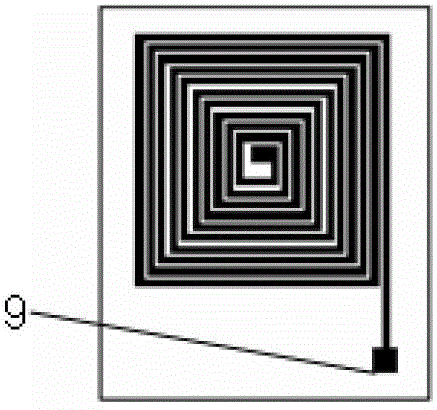
[0026] The inductance coil structure of the micro sensor of the present invention is based on the comparison of self-inductance and mutual inductance. Considering that the inductance coil in the self-inductance structure acts as an excitation and a detection coil at the same time, the signal-to-noise ratio is small in practical applications, so the present invention Select the mutual inductance structure, that is, the sensor is composed of independent detection coils and excitation coils. The alternating current generated by the signal source is applied to the excitation coil, and the generated alternating electric field makes the surface of the workpiece under test in an alternating magnetic field, thereby inducing eddy currents; the adjacent detection coils form a reverse spiral, and pass between the coils The wire columns are connected in series, ...


PUM

PropertyMeasurementUnit
thicknessaaaaaaaaaa

Abstract

The invention relates to a miniature eddy current sensor with a structure consisting of a silicon substrate and multilayer coils, and belongs to the field of miniature sensors. The miniature eddy current sensor is used for detecting micro-cracks on surfaces of metal components, is based on the three-inch silicon substrate with the thickness of 200 micrometers and comprises a single-layer excitation coil, multiple layers of detection coils, conducting layers and insulating layers, each two layers of detection coils are serially connected and communicated by a central lead in a reverse spiral surrounding manner, flow directions of induced currents of the detection coils are consistent assuredly, and detection signals are intensified; and each silica insulating layer is filled between the corresponding detection coil and the excitation coil. The size of the section of each detection coil can be 10 micrometers X 10 micrometers, 20 micrometers X 15 micrometers and 30 micrometers X 15 micrometers, each coil includes 10 turns, the corresponding size of the section of the excitation coil can be 140 micrometers X 20 micrometers, 290 micrometers X 20 micrometers and 430 micrometers X 20 micrometers, and the excitation coil includes a single turn. The inductance coils are squarely or circularly spiral in a planar manner, and are distributed in a matrix manner according to the shapes and the sizes of the inductance coils, so that detection area is increased, and detection efficiency is improved. By the aid of via UV-LIGA (ultraviolet-lithography) which is precision processing technology on the basis of a micro-electro-mechanical system MEMS, the miniature eddy current sensor has the advantages of slim structure, miniaturization and high sensitivity and efficiency, and is applicable to nondestructive detection of microdefects on surfaces of metal workpieces.

Description

technical field [0001] The invention belongs to the technical field of microsensors, and in particular relates to the detection of tiny cracks on the surface of metal components. Background technique [0002] At present, the equipment used for non-destructive testing of micro-cracks mainly consists of magnetic particle flaw detectors, ultrasonic flaw detectors, and ray flaw detectors. [0003] Magnetic particle flaw detectors have certain disadvantages: for example, the detection sensitivity of micro-cracks on the surface is relatively low, and it is difficult to find defects; it is necessary to pre-treat the surface of the workpiece before detection to remove grease, paint and rust on the surface, which greatly increases the preparation time; The measured workpiece is easily magnetized. After the detection, it needs to be demagnetized and the magnetic powder is removed. The detection efficiency is low and the detection cycle is prolonged. [0004] In addition to some of th...

Claims


Application Information

Patent Timeline
Patent Type & Authority Applications(China)
IPC IPC(8): G01N27/90
Inventor 徐志祥姜凤娟尹嘉鹏孙浩
Owner DALIAN UNIV OF TECH
Learn More