Groove-gate semiconductor power device

A technology for power devices and semiconductors, applied in semiconductor devices, electrical components, circuits, etc., can solve problems such as the inability to play the role of high-K dielectrics, alleviate the problem of charge imbalance, increase flexibility, increase withstand voltage and process tolerances Effect

Active Publication Date: 2015-06-10
UNIV OF ELECTRONICS SCI & TECH OF CHINA
View PDF4 Cites 0 Cited by
  • Summary
  • Abstract
  • Description
  • Claims
  • Application Information

AI Technical Summary

Problems solved by technology

[0009] The purpose of the present invention is to overcome the shortcoming that current semiconductor devices cannot play the role of high-K dielectric in the case of relatively large spacing and small density of dielectric grooves, and provide a groove-gate semiconductor power device

Method used


Image

  • Groove-gate semiconductor power device
  • Groove-gate semiconductor power device
  • Groove-gate semiconductor power device

Examples


Embodiment

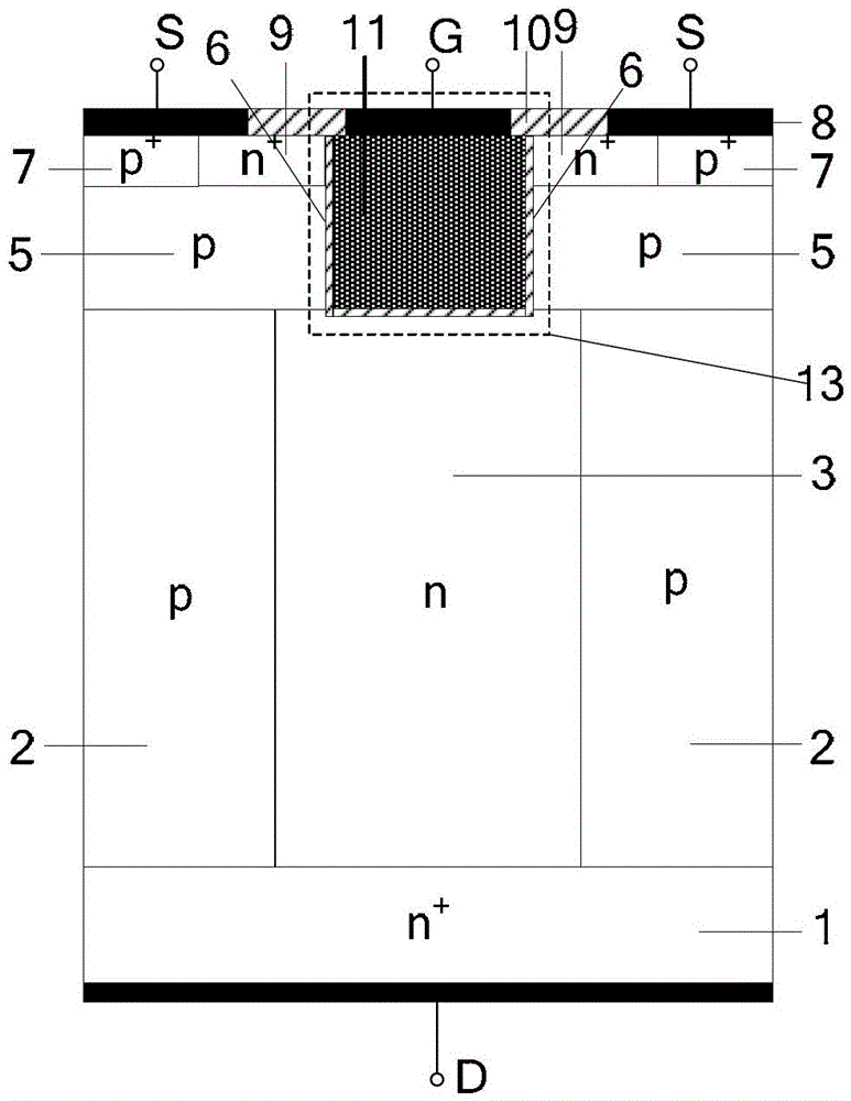
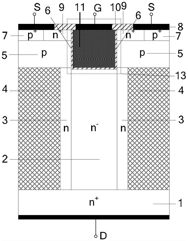
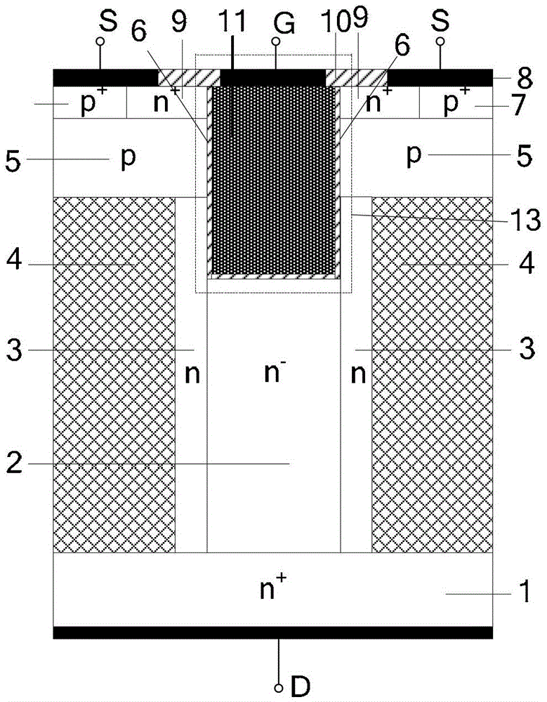
[0032] In this example, an N-channel trench-gate VDMOS device with a low-resistance current channel is taken as an example. The cross-sectional view is as follows figure 2 . In the case of N-channel VDMOS devices the semiconductor substrate is n + Type doping (that is, n-type dielectric with doping concentration greater than n-type doping concentration).

[0033] The slot-gate semiconductor power device in this example includes n + Type-doped semiconductor substrate 1, trench gate structure 13, active region, semiconductor drift region and two high-K dielectric regions 4, the semiconductor drift region includes a first semiconductor region 2 and two second semiconductor regions 3, the first The semiconductor region 2 is arranged above the semiconductor substrate 1, the two second semiconductor regions 3 are arranged above the semiconductor substrate 1, the high-K dielectric region 4 is arranged above the semiconductor substrate 1, and the two sides of the first semiconducto...


PUM


Abstract

A trench-gate semiconductor power device, which adds two high-K dielectric regions (4) at the left side and the right side of a semiconductor drift region, wherein the two sides of a first semiconductor region (2) in the semiconductor drift region are in contact with two second semiconductor regions (3), and the two high-K dielectric regions (4) are respectively in contact with the other sides of the two second semiconductor regions (3), thereby solving the problem that the existing semiconductor device cannot exert the high-K dielectric function in the case of relatively wide spacing and small density of dielectric trenches, and enabling the reduction of the specific on-resistance, the increase of the voltage resistance, and the application to an MOS device or an MOS controlled semiconductor device.

Description

technical field [0001] The invention relates to semiconductor technology, in particular to a low-power semiconductor power device with a dielectric groove and a groove gate structure. Background technique [0002] The high voltage resistance of power MOSFET (metal oxide semiconductor Field-Effect Transistor) requires a long drift region and low doping concentration in the drift region, which makes the ratio of on-resistance R on,sp Press R according to the device withstand voltage BV on,sp ∝BV 2.3~2.6 The relationship increases, resulting in increased power consumption. [0003] The specific on-resistance drop of the planar gate VDMOS (vertical double diffusion metal oxide semiconductor, vertical double diffusion metal-oxide-semiconductor field effect transistor) has reached its limit due to the limitation of the JFET (junction field-effect transistor) effect. Since the UMOS (U-type trench MOS, U-type trench MOS) structure has no JFET effect and high channel density, its ...

Claims


Application Information

Patent Timeline
Patent Type & Authority Patents(China)
IPC IPC(8): H01L29/06H01L29/78
CPCH01L29/7813H01L29/0634H01L29/0653H01L29/0878H01L29/7397
Inventor 罗小蓉蒋永恒蔡金勇范叶王沛王骁伟周坤王琦罗尹春张波
Owner UNIV OF ELECTRONICS SCI & TECH OF CHINA
Why Eureka
Try Eureka