Trench type semiconductor power device

一种半导体、器件的技术,应用在低功耗半导体功率器件领域,能够解决工艺成本高、增加工艺复杂度、工艺难度大等问题,达到避免复杂工艺、增加漂移区浓度、大灵活性的效果

Inactive Publication Date: 2011-06-29
UNIV OF ELECTRONICS SCI & TECH OF CHINA
View PDF9 Cites 31 Cited by
  • Summary
  • Abstract
  • Description
  • Claims
  • Application Information

AI Technical Summary

Problems solved by technology

But there are still disadvantages: (1) Since the device structure in this patent is obtained based on some conventional processes, the process is relatively difficult and the process cost is high, and the P column area and the N column area cannot be made very narrow (rather than the conduction It cannot be made very small); (2) Since the structure in this patent is based on a conventional process, if you want to use high-K dielectrics to improve performance, you generally need to make independent grooves, which will inevitably increase the complexity of the process

Method used


Image

  • Trench type semiconductor power device
  • Trench type semiconductor power device
  • Trench type semiconductor power device

Examples


Embodiment Construction

[0041] The present invention will be described in detail below in conjunction with the accompanying drawings.

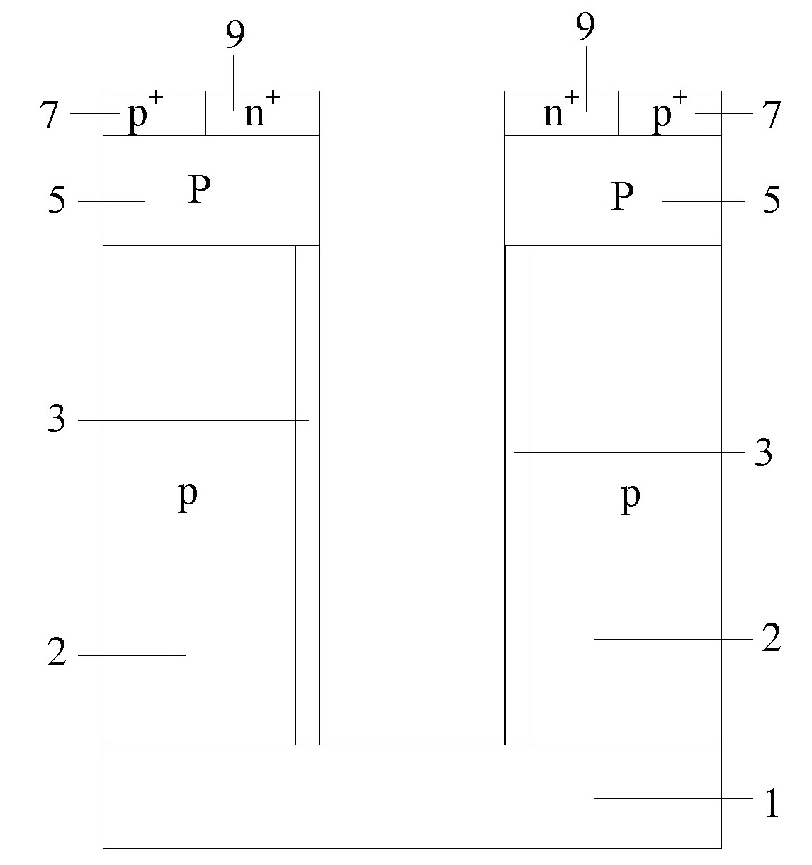
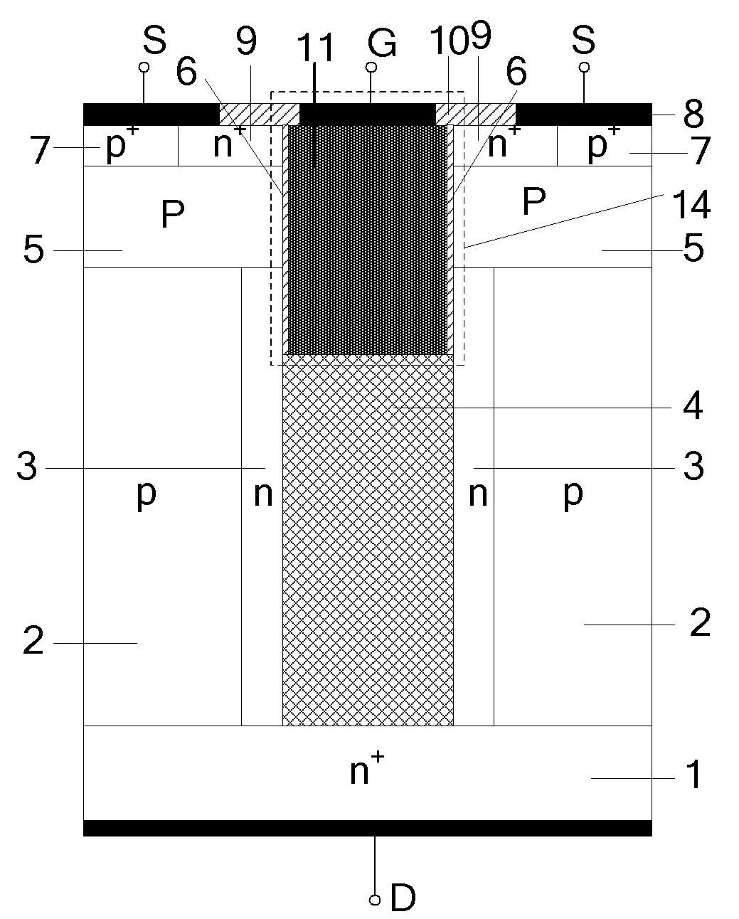
[0042] Conventional trench-gate VDMOS structure with superjunction, such as figure 1 As shown, on the semiconductor substrate 1 is a drift region, the drift region includes alternating p-type semiconductor regions 2' and n-type semiconductor regions 3', the p-type semiconductor regions 2' and n-type semiconductor regions 3' are columnar, and also Referred to as a p-column region and an n-column region, the p-type semiconductor region 2' and the n-type semiconductor region 3' form a super junction structure. The n-type semiconductor region 3' is located directly below the groove gate structure 14, and the width of the n-type semiconductor region 3' is greater than the width of the groove gate structure. The groove gate structure includes a gate dielectric 6 and a conductive material 11 surrounded by the gate dielectric. From the surface of the conductive material 11 ...


PUM


Abstract

The invention relates to a semiconductor device. The device comprises a semiconductor substrate, a semiconductor drift region on the semiconductor substrate, a high-K dielectric on the semiconductor substrate, an active region on the semiconductor drift region and a trench gate structure on the high-K dielectric, wherein the semiconductor drift region comprises a first conduction type semiconductor region and a second conduction type semiconductor region which form a super-junction structure; the high-K dielectric is adjacent to the second conduction type semiconductor region; the trench gate structure is adjacent to the active region; and the second conduction type semiconductor region is formed through ion implantation at a small inclination angle, so that the semiconductor device is narrow and has high concentration.

Description

technical field [0001] The invention relates to a semiconductor power device, in particular to a low power consumption semiconductor power device with a groove gate structure. Background technique [0002] Power MOSFET (metal oxide semiconductor Field-Effect Transistor) is a multi-subconduction device with high input impedance, easy driving, fast speed, high frequency, positive temperature coefficient of on-resistance, wide safe operating area, and parallel use, etc. advantage. These advantages make it widely used in industrial control, aerospace, communications, automobiles, computers and portable appliances, home appliances, office supplies and other fields, especially in the application of switching power supplies, which has achieved rapid development and greatly improved the efficiency of electronic systems . [0003] The high voltage resistance of the device requires a long drift region and a low doping concentration in the drift region. However, as the length of the...

Claims


Application Information

Patent Timeline
Patent Type & Authority Applications(China)
IPC IPC(8): H01L29/78H01L29/06H01L29/51
CPCH01L29/0634H01L29/7813H01L29/0878H01L29/7397H01L29/0653H01L21/26586H01L29/66734H01L29/0886
Inventor 罗小蓉姚国亮雷天飞王元刚张波
Owner UNIV OF ELECTRONICS SCI & TECH OF CHINA
Why Eureka
Try Eureka