
Silicon nitride film preparation device

A technology for preparing a device and a silicon nitride film, which is applied in gaseous chemical plating, metal material coating process, coating, etc., can solve problems such as increased production costs, substandard products, and difficulty in ensuring product quality, and achieves improved product quality. quality effect

Inactive Publication Date: 2012-10-17
LESHAN TOPRAYCELL
View PDF3 Cites 8 Cited by
  • Summary
  • Abstract
  • Description
  • Claims
  • Application Information

AI Technical Summary

Problems solved by technology

This kind of silicon nitride film preparation device has the following problems in the actual use process: because different process gases have different densities, it is difficult to mix them evenly by free diffusion after the various process gases are passed into the vacuum deposition chamber, This will cause differences in the gas composition and the concentration of each component in the vacuum deposition chamber. For example, the concentration of ammonia gas in some places is relatively high, and the concentration of ammonia hydride in some places is relatively high, which will lead to silicon wafers in different places in the vacuum deposition chamber. The composition and film thickness of the silicon nitride deposited on the surface are different, so it is difficult to guarantee the product quality. Moreover, after the process gas enters from the front end of the vacuum deposition chamber, the process gas is quickly pumped into the vacuum deposition chamber under the action of the vacuum pump. The tail end of the chamber is discharged from the exhaust hole, so that there is less gas at the front end of the vacuum deposition chamber, so that the silicon nitride film formed on the surface of the silicon wafer at the front end is thinner, while a large amount of silicon nitride film is accumulated at the tail end of the vacuum deposition chamber. The gas makes the silicon nitride film formed on the surface of the silicon wafer at the tail end thicker, so that there will be a large number of unqualified products, which makes the production efficiency lower and the production cost will be greatly increased.

Method used


Image

  • Silicon nitride film preparation device

Examples


Embodiment Construction

[0015] The present invention will be further described below in conjunction with the accompanying drawings.

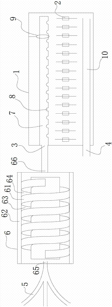
[0016] like figure 1 As shown, the silicon nitride film preparation device includes a vacuum deposition chamber 1, a plurality of plasma reactors 2 are arranged in the vacuum deposition chamber 1, an air inlet 3 and an air extraction port 4 are arranged on the vacuum deposition chamber 1, and the inlet The gas port 3 is connected with a gas mixing device, the gas mixing device is provided with an inlet 65 and an outlet 66, and the inlet 65 is connected with a plurality of inlet pipes 5 for feeding process gas, and the outlet 66 is connected with the vacuum The gas inlet 3 of the deposition chamber 1 communicates. By connecting the gas mixing device to the gas inlet 3 of the vacuum deposition chamber 1, before various process gases enter the vacuum deposition chamber 1, the gas mixing device is used to mix the various process gases to make them evenly mixed, and then ...


PUM


Abstract

The invention provides a silicon nitride film preparation device, which can evenly mix gases of various manufacture procedures. The silicon nitride film preparation device comprises a vacuum deposition chamber, wherein a plurality of plasma reactors are arranged in the vacuum deposition chamber; the vacuum deposition chamber is provided with a gas inlet and a bleeding point; the air inlet is connected with a gas mixing device; the gas mixing device is provided with an inlet and an outlet; the inlet is connected with a plurality of air inlet pipes used for introducing in manufacture procedure gas; and the outlet is communicated with the air inlet of the vacuum deposition chamber. Firstly, the gases of various manufacture procedures are mixed by the gas mixing device; after the gases are evenly mixed, the gases are introduced into the vacuum deposition chamber to react; therefore, the components and the component concentrations of various gases in the vacuum deposition chamber are same; the component and the membrane thickness of silicon nitride deposited on the surfaces of wafers on different positions in the vacuum deposition chamber tend to be similar; and the product quality can be greatly improved. The silicon nitride film preparation device disclosed by the invention is suitable for popularizing and applying in the crystalline silicon solar energy production equipment field.

Description

technical field [0001] The invention relates to the field of crystalline silicon solar energy production equipment, in particular to a silicon nitride film preparation device. Background technique [0002] Since the sunlight is irradiated on the silicon wafer of the solar cell, part of the sunlight will be reflected. Even if the silicon surface is designed as a suede surface, although the incident light will produce multiple reflections to increase the light absorption rate, there will still be Part of the sunlight will be reflected. In order to reduce the reflection loss of sunlight, the usual method is to cover a layer of anti-reflection film on the surface of the silicon wafer of the solar cell. This film can reduce the reflectivity of sunlight and increase the photoelectric conversion. Efficiency, in the technology of depositing anti-reflection film on the surface of crystalline silicon, silicon nitride film has the characteristics of high insulation, good chemical stabi...

Claims


Application Information

Patent Timeline
Patent Type & Authority Applications(China)
IPC IPC(8): C23C16/34C23C16/455C23C16/50
Inventor 陈五奎李军徐文州耿荣军查恩
Owner LESHAN TOPRAYCELL
Learn More