Wafer temporary bonding method

A temporary bonding and wafer technology, applied in the field of bonding, can solve the problems of long polishing time, residual slurry pollution, increased production costs, etc., and achieve the effect of avoiding the influence of warpage, convenient operation and reducing the influence

Active Publication Date: 2012-10-24
JIANGSU R & D CENTER FOR INTERNET OF THINGS
View PDF1 Cites 11 Cited by
  • Summary
  • Abstract
  • Description
  • Claims
  • Application Information

AI Technical Summary

Problems solved by technology

However, the use of chemical mechanical polishing (CMP) is prone to contamination of residual slurry, and the polishing time used is longer, which increases production costs

Method used


Image

  • Wafer temporary bonding method
  • Wafer temporary bonding method
  • Wafer temporary bonding method

Examples


Embodiment Construction

[0027] The present invention will be further described below in conjunction with specific drawings and embodiments.

[0028] In order to be able to reduce the impact of warpage on devices after wafer thinning, the present invention uses a temporary bonding method to form a permanent bonding process. Specifically, the temporary wafer bonding method of the present invention includes the following steps:

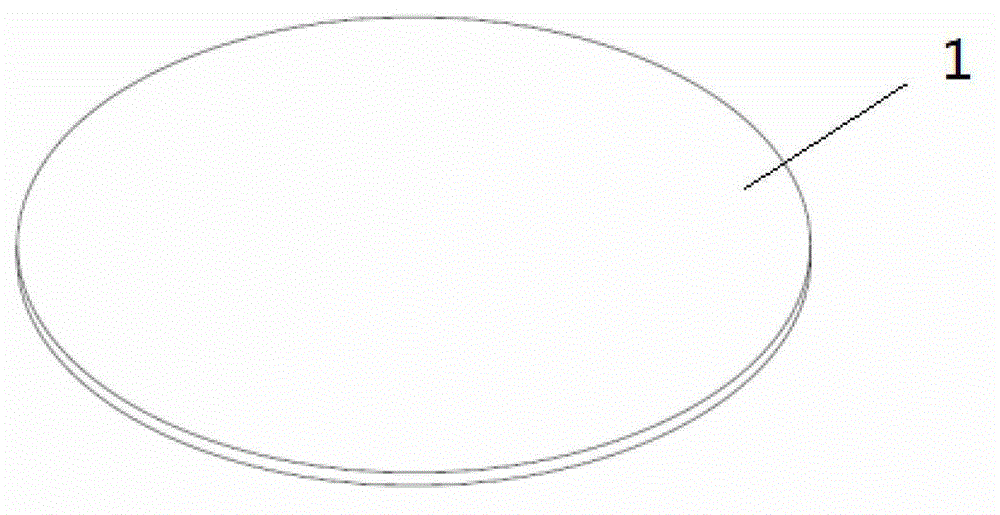
[0029] a. Provide and clean the required first wafer 1 to be bonded;

[0030] like figure 1 As shown: the material of the first wafer 1 includes silicon and germanium, and the first wafer 1 may also use SOI (silicon on insulator);

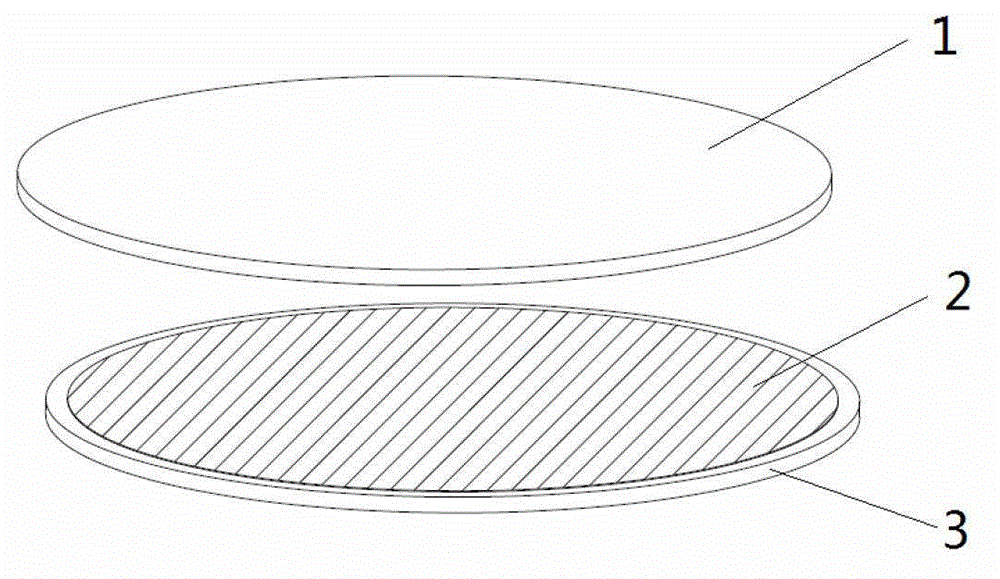
[0031] b. Provide a carrier wafer 2, and spin-coat an adhesive 3 on a surface of the carrier wafer 2;

[0032] like figure 2 As shown: the carrier wafer 2 is a transitional wafer, and the adhesive 3 is made of conventional materials, such as SU-8, etc., which will not be listed here;

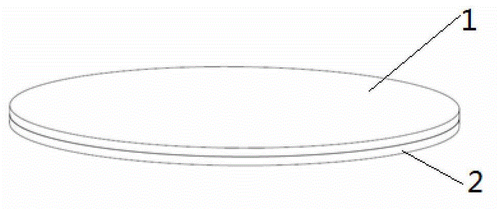
[0033] c. Transfer the above-mentioned first wafer 1 and ca...


PUM


Abstract

The invention relates to a wafer temporary bonding method, which comprises the following steps of: a, providing and washing a first wafer; b, providing a carrier wafer, and spin-coating a bond; c, transferring the first wafer and the carrier wafer into a bonding box to form a first bonding body, and thinning the first wafer on the first bonding body according to demands; d, scribing the thinned first wafer on the first bonding body by utilizing a laser scribing machine; e, transferring the first bonding body into the bonding box, and enabling the temperature inside the bonding box to be higher than a softening temperature of the bond; and uniformly applying pressure on the surface of the first wafer by utilizing a flat wafer in the bonding box; f, providing a needed second wafer, and bonding the second wafer with the first wafer according to demands to form a second bonding body; and g, de-bonding the second bonding body. The technique steps are convenient to operate, the production cost is reduced, the tilt curvature influence after the thinning of the wafer can be avoided, permanent bonding can be formed, and safety and reliability can be realized.

Description

technical field [0001] The invention relates to a bonding method, in particular to a wafer temporary bonding method, specifically a method for solving the influence of substrate warpage on wafer bonding, and belongs to the technical field of semiconductors. Background technique [0002] Wafer bonding technology refers to the method of tightly combining two wafers through chemical and physical effects. Wafer bonding is often combined with surface silicon processing and bulk silicon processing, and is used in the processing technology of MEMS. Although wafer bonding is not a direct means of micromachining, it plays an important role in micromachining. By combining with other processing methods, it can not only provide support and protection for microstructures, but also realize the mechanical structure between mechanical structures or mechanical structures. An electrical connection to a circuit. The quality of wafer bonding will have a direct impact on the performance of the ...

Claims


Application Information

Patent Timeline
Patent Type & Authority Applications(China)
IPC IPC(8): H01L21/603
Inventor 张昕欧文明安杰谭振新
Owner JIANGSU R & D CENTER FOR INTERNET OF THINGS
Why Eureka
Try Eureka