
Tunable semiconductor laser unit

A laser and semiconductor technology, applied in semiconductor lasers, lasers, laser parts, etc., can solve the problem of inconsistent output optical power, and achieve the effects of fast wavelength dynamic switching, easy fabrication, and narrow spectral line width.

Active Publication Date: 2014-09-03
HUAZHONG UNIV OF SCI & TECH
View PDF3 Cites 0 Cited by
  • Summary
  • Abstract
  • Description
  • Claims
  • Application Information

AI Technical Summary

Problems solved by technology

[0010] The object of the present invention is to provide a tunable semiconductor laser, which can improve the inconsistency of the output optical power of each wavelength channel when the existing laser is tuned, and can realize wide wavelength range tuning and fast wavelength switching. The grating area can use very Manufactured by mature holographic exposure method, which has the advantage of simple process

Method used


Image

  • Tunable semiconductor laser unit
  • Tunable semiconductor laser unit
  • Tunable semiconductor laser unit

Examples


Embodiment 1

[0051]In the first implementation example, the front and rear Bragg gratings 9 and 10 all adopt two sets of interleaved multi-phase shift sampling gratings, with Figure 5 It is a schematic structural diagram of the front and rear interleaved multi-phase-shift sampling gratings of the first implementation example, and from top to bottom are the first and second groups of multi-phase-shift sampling gratings. For the front and rear Bragg gratings 9, 10, according to the formula m=2, i=1, 2. The grating initial phase difference between adjacent sampling periods of the first group of multi-phase shift sampling gratings is The grating initial phase difference between adjacent sampling periods of the second group of multi-phase shift sampling gratings is The two sets of interleaved multi-phase-shift sampling gratings have the same grating period and sampling period. See the dotted arrow in the direction from the second group of multi-phase-shift sampling gratings to the first ...

Embodiment 2

[0056] In the second implementation example, the front and rear Bragg gratings 9 and 10 all adopt three sets of interleaved multi-phase shift sampling gratings, with Figure 9 It is a schematic structural diagram of the front and rear interleaved multi-phase shift sampling gratings of the second implementation example. From top to bottom are the second, first and third groups of multi-phase shift sampling gratings respectively. For the front and rear Bragg gratings 9, 10, according to the formula m=3, i=1, 2, 3. The grating initial phase difference between adjacent sampling periods of the first group of multi-phase shift sampling gratings is The grating initial phase difference between adjacent sampling periods of the second group of multi-phase shift sampling gratings is The grating initial phase difference between adjacent sampling periods of the third group of multi-phase shift sampling gratings is The second and third groups of multi-phase-shift sampling gratings ar...


PUM


Abstract

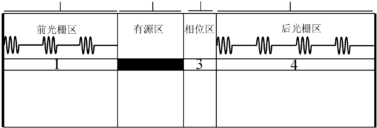
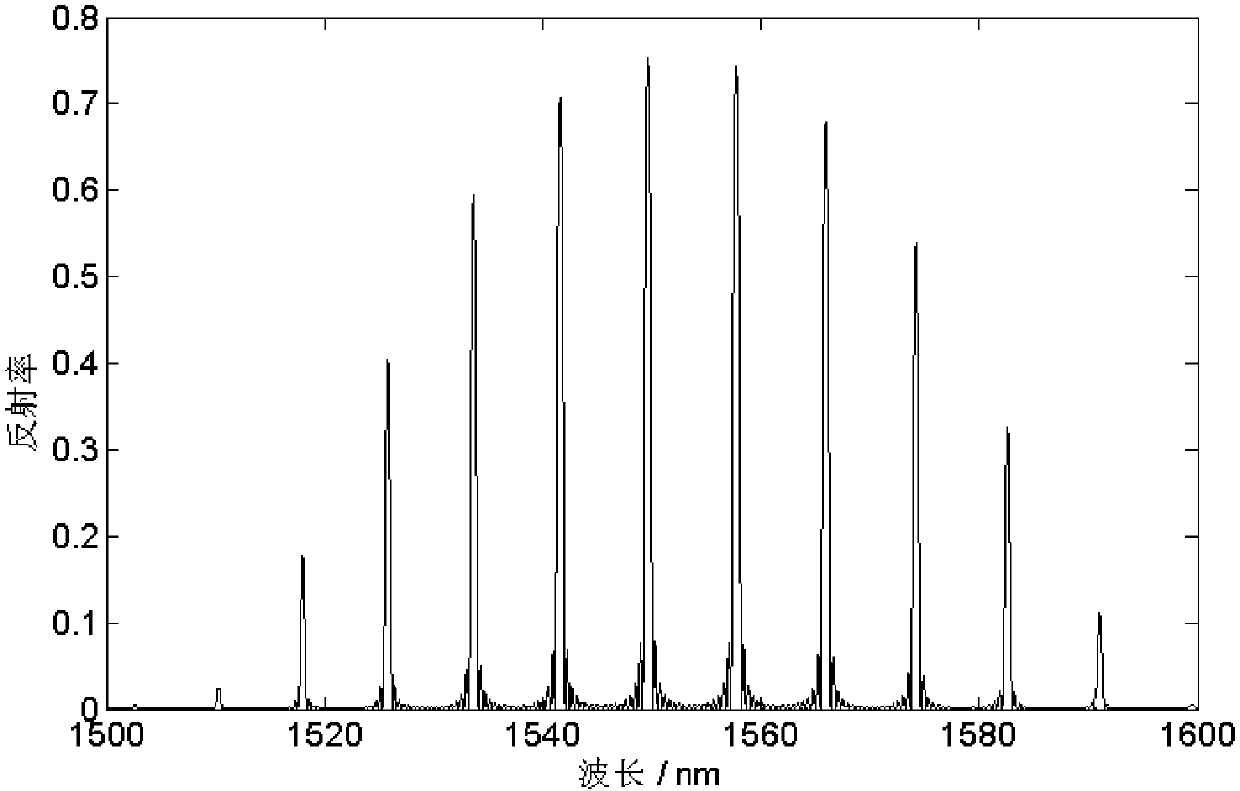
The invention discloses a tunable semiconductor laser unit which is composed of a front grating area, an active area, a phase area and a rear grating area, wherein the front grating area and the rear grating area are designed into a novel Bragg grating; the grafting is used or generating a comb reflection response with a balanced reflective peak, and a reflective index value of the grating area is changed by injecting current to the front grating and the rear grating by the vernier caliper effect so as to achieve quasi continuous tuning of a wide spectrum. The laser unit has the advantages that the output optical power is high; the optical power uniformity of each channel is good, and the switching speed of dynamic wavelength is high. Two Bragg reflection sections of the laser unit can also be designed into various apodisation and chirping forms of the Bragg grating. The laser unit also can be integrated with apparatuses such as a semiconductor light amplifier and an electro-absorption modulator.

Description

technical field [0001] The invention relates to a tunable semiconductor laser, which belongs to the field of laser technology. The laser is a Bragg reflection laser based on interleaved multi-phase-shift sampling gratings. Background technique [0002] With the development of optical communication, especially the continuous development of optical communication network, research on Dense Wavelength Division Multiplexing (DWDM) technology and even Wavelength Division Multiplexing (WDM) / Optical Time Division Multiplexing (OTDM) system has achieved rapid development. , so there is a higher challenge to the flexibility of the light source and the system. A tunable semiconductor laser can replace multiple fixed-wavelength lasers, thus reducing the manufacturing cost of the laser, simplifying the module packaging process, and reducing the cost of backup and inventory management; in optical network systems, the wavelength of the tunable laser can be adjusted The performance can all...

Claims


Application Information

Patent Timeline
Patent Type & Authority Patents(China)
IPC IPC(8): H01S5/125
Inventor 赵家霖余永林
Owner HUAZHONG UNIV OF SCI & TECH
Learn More