

Single particle irradiation-resistant super junction VDMOS device
An anti-single event radiation and device technology, applied in semiconductor devices, electrical components, circuits, etc., can solve problems such as VDMOS burnout
- Summary
- Abstract
- Description
- Claims
- Application Information
AI Technical Summary
Problems solved by technology
Method used
Image


Examples
Embodiment Construction
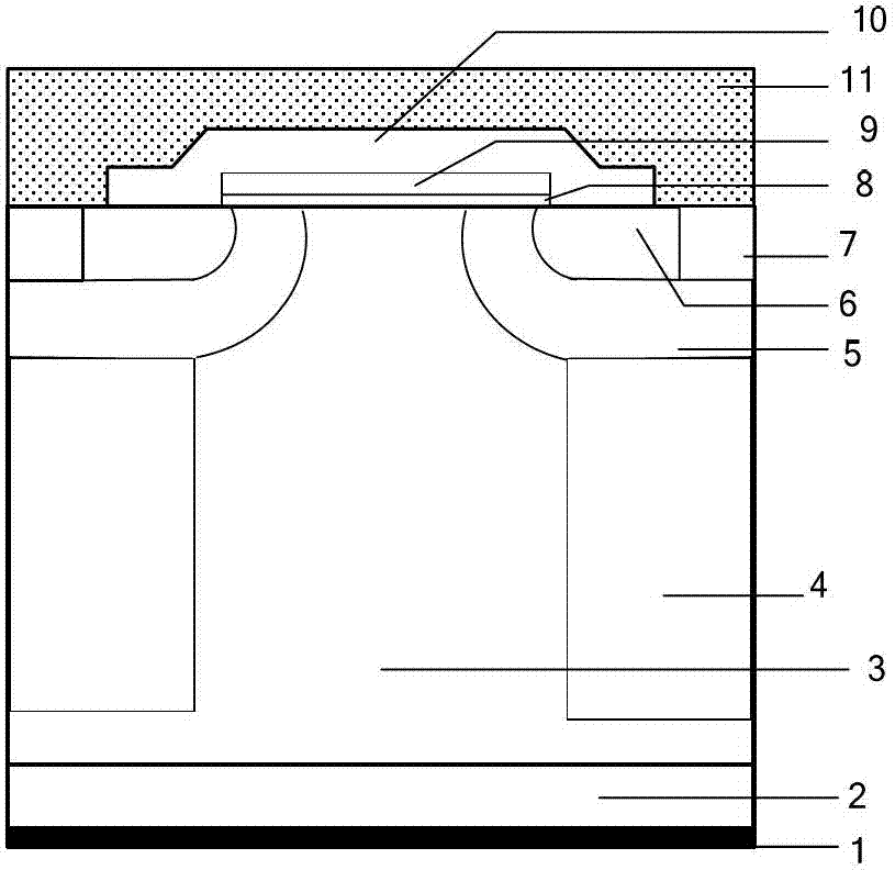
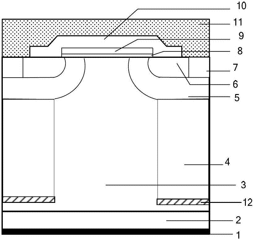
[0021] A super-junction VDMOS device resistant to single-event irradiation, the basic structure of which is shown in Figures 2a to 2c, including a heavily doped semiconductor substrate 2 of the first conductivity type, located on the back of the heavily doped semiconductor substrate 2 of the first conductivity type The metallized drain electrode 1, the lightly doped semiconductor epitaxial layer 3 of the first conductivity type located on the front surface of the heavily doped semiconductor substrate 2 of the first conductivity type; the top two sides of the lightly doped semiconductor epitaxial layer 3 of the first conductivity type respectively have A second conductivity type semiconductor base region 5, each second conductivity type semiconductor base region 5 respectively has a first conductivity type heavily doped semiconductor source region 6 and a second conductivity type heavily doped semiconductor body region 7; Both the heavily doped semiconductor source region 6 of t...
PUM
 Abstract
Description
Claims
Application Information