Composite Source Field Plate Current Aperture Heterojunction Field Effect Transistor

A technology of heterojunction field effect and source field plate, which is applied in the field of microelectronics, can solve the problems that the field plate structure cannot effectively modulate the electric field distribution in the device, and the performance of the device has not been improved, so as to avoid the problem of process complexity and improve breakdown voltage, easy-to-achieve effects

Active Publication Date: 2020-06-16
XIDIAN UNIV
View PDF7 Cites 0 Cited by
  • Summary
  • Abstract
  • Description
  • Claims
  • Application Information

AI Technical Summary

Problems solved by technology

However, up to now, there is still no precedent of the field plate structure being successfully applied to GaN-based current aperture heterojunction field effect devices at home and abroad. This is mainly due to the inherent defects in the structure of GaN-based current aperture heterojunction field effect devices. As a result, the strongest electric field peak in the device drift layer is located near the interface between the current blocking layer and the aperture layer, and the electric field peak is far away from the surfaces on both sides of the drift layer, so the field plate structure can hardly play the role of effectively modulating the electric field distribution in the device, even in GaN The field plate structure is used in the base current aperture heterojunction field effect device, and there is almost no improvement in device performance

Method used


Image

  • Composite Source Field Plate Current Aperture Heterojunction Field Effect Transistor
  • Composite Source Field Plate Current Aperture Heterojunction Field Effect Transistor
  • Composite Source Field Plate Current Aperture Heterojunction Field Effect Transistor

Examples


Embodiment 1

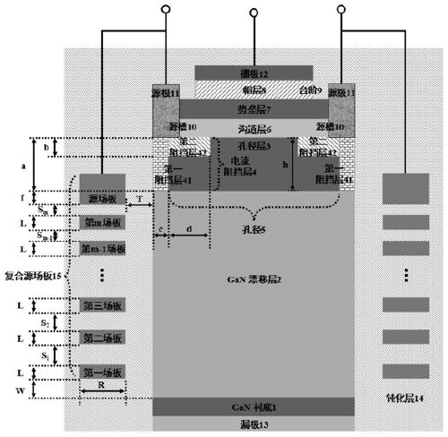
[0067] Embodiment 1: Fabrication of a composite source field plate current aperture heterojunction field effect transistor with SiN as the passivation layer and 2 floating field plates.

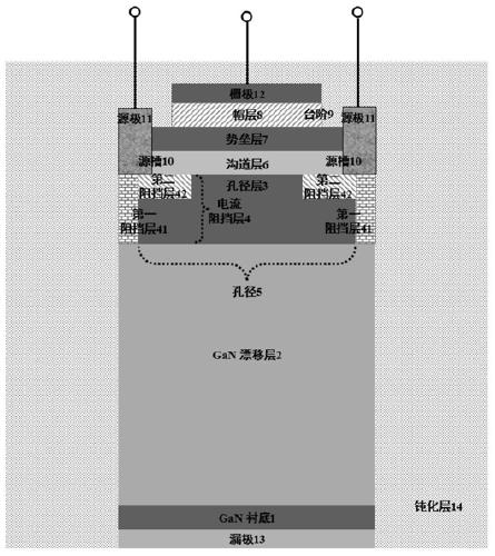
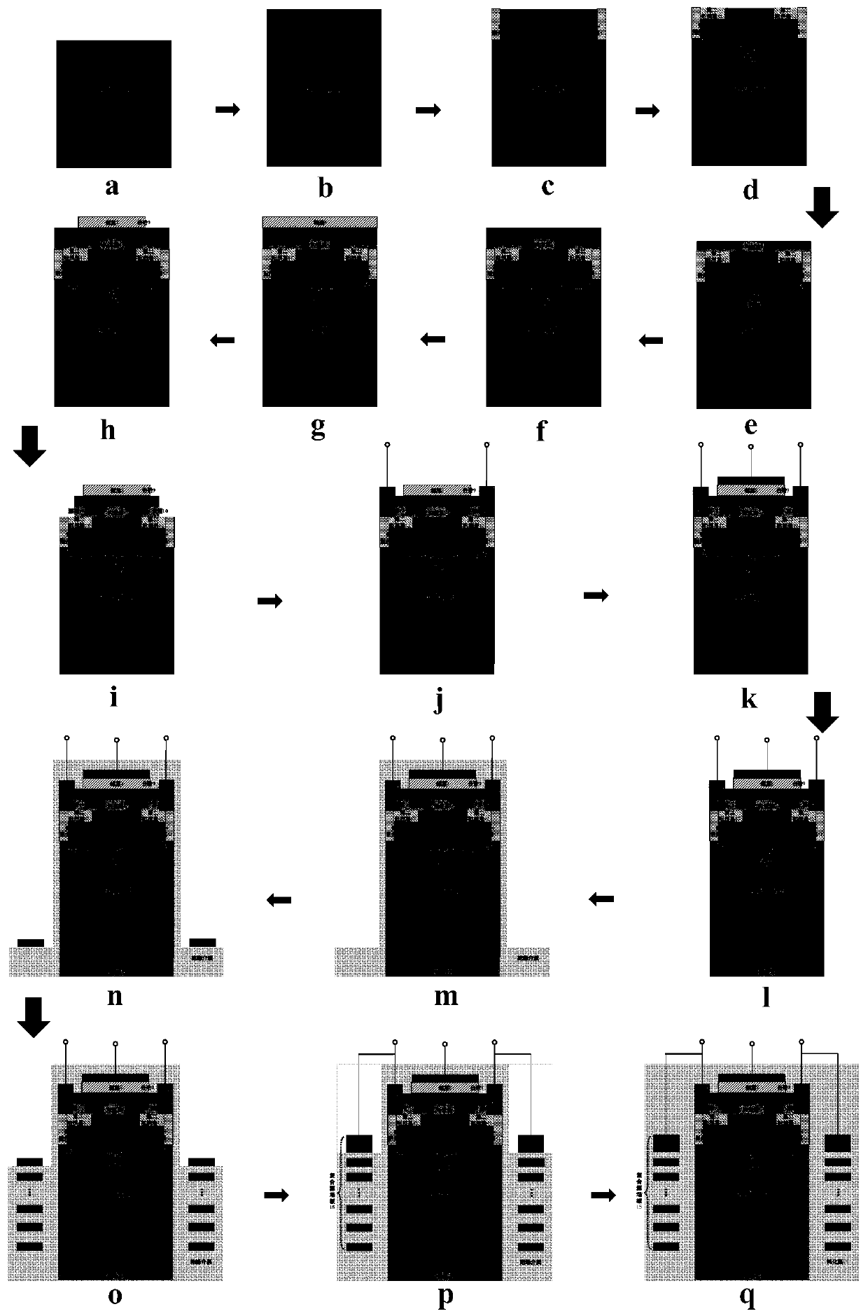
[0068] Step 1. Epitaxy n on GaN substrate 1 - Type GaN, forming a GaN drift layer 2, such as image 3 a.

[0069] Use n + Type GaN is used as the GaN substrate 1, using metal organic chemical vapor deposition technology, and the epitaxial doping concentration on the GaN substrate 1 is 1×10 15 cm -3 N - Type GaN semiconductor material to form a GaN drift layer 2, where:

[0070] The process conditions used for epitaxy are: temperature is 950℃, pressure is 40 Torr, and SiH 4 As the doping source, the hydrogen flow rate is 4000 sccm, the ammonia flow rate is 4000 sccm, and the gallium source flow rate is 100 μmol / min.

[0071] Step 2. Epitaxy n-type GaN on the GaN drift layer 2 to form the aperture layer 3, such as image 3 b.

[0072] Using metal organic chemical vapor deposition technology, the epitaxia...

Embodiment 2

[0130] Example 2: Making passivation layer as SiO 2 , And the number of floating field plates is 2 composite source field plate current aperture heterojunction field effect transistor.

[0131] Step 1. Epitaxy n on GaN substrate 1 - Type GaN, forming a GaN drift layer 2, such as image 3 a

[0132] At a temperature of 950℃, a pressure of 40 Torr, and SiH 4 As the doping source, the hydrogen flow rate is 4000 sccm, the ammonia flow rate is 4000 sccm, and the gallium source flow rate is 100 μmol / min. + The type GaN material is used as the GaN substrate 1, using metal organic chemical vapor deposition technology, and the epitaxial doping concentration on the GaN substrate 1 is 5.5×10 16 cm -3 N - Type GaN material to complete the production of the GaN drift layer 2.

[0133] Step 2. Epitaxy n-type GaN on the GaN drift layer 2 to form the aperture layer 3, such as image 3 b.

[0134] At a temperature of 1000°C, a pressure of 45 Torr, and SiH 4 As the doping source, the hydrogen flow rate ...

Embodiment 3

[0177] Embodiment 3: Fabrication of a composite source field plate current aperture heterojunction field effect transistor whose passivation layer is SiN and the number of floating field plates is 3.

[0178] Step A. Use a temperature of 950℃, a pressure of 40 Torr, and SiH 4 As the doping source, the hydrogen flow rate is 4000 sccm, the ammonia flow rate is 4000 sccm, and the gallium source flow rate is 100 μmol / min. + Type GaN material is used as the GaN substrate 1, using metal organic chemical vapor deposition technology, and the epitaxial doping concentration on the GaN substrate is 1×10 18 cm -3 N - Type GaN material to make GaN drift layer 2, such as image 3 a.

[0179] Step B. Use a temperature of 950℃, a pressure of 40 Torr, and SiH 4 As the doping source, the hydrogen flow rate is 4000 sccm, the ammonia flow rate is 4000 sccm, and the gallium source flow rate is 100 μmol / min. Using metal organic chemical vapor deposition technology, the epitaxial thickness on the GaN drift...


PUM

PropertyMeasurementUnit
thicknessaaaaaaaaaa
widthaaaaaaaaaa
thicknessaaaaaaaaaa

Abstract

The invention discloses a composite source field plate-based current aperture heterojunction field effect transistor. The heterojunction field effect transistor comprises a drain (13), a GaN substrate (1), a GaN drifting layer (2), an aperture layer (3), two symmetrical two-stage-step-shaped current blocking layers (4), a channel layer (6), a barrier layer (7), a cap layer (8) and a gate (12) from the bottom up; source grooves (10) are etched in the two sides of the channel layer and the barrier layer; two sources (11) are deposited in the source grooves; two steps (9) are etched in the two sides of the cap layer; all regions, except the drain bottom, are covered with a passivation layer (14); a composite source field plate is manufactured in the passivation layer on the two sides; the composite source field plate consists of multiple mutually-independent floating field plates and a source field plate; the source field plate is electrically connected with the sources; and an aperture (5) is formed between the two current blocking layers (4). The heterojunction field effect transistor has high breakdown voltage, simple process, low conduction resistance and high rate of finished products, and can be used for a power electronic system.

Description

Technical field [0001] The invention belongs to the field of microelectronics technology, and relates to semiconductor devices, especially composite source field plate current aperture heterojunction field effect transistors, which can be used in power electronic systems. [0002] technical background [0003] Power semiconductor devices are the core components of power electronic technology. As energy and environmental issues become increasingly prominent, the development of new high-performance, low-loss power devices has become one of the effective ways to improve power utilization, save energy, and alleviate energy crises. In the research of power devices, there is a serious restriction relationship between high speed, high voltage and low on-resistance. A reasonable and effective improvement of this restriction relationship is the key to improving the overall performance of the device. With the development of microelectronics technology, the performance of traditional first-ge...

Claims


Application Information

Patent Timeline
Patent Type & Authority Patents(China)
IPC IPC(8): H01L29/40H01L29/778H01L29/06H01L21/335
CPCH01L29/0615H01L29/404H01L29/66462H01L29/7787
Inventor 毛维杨翠马佩军郝跃
Owner XIDIAN UNIV
Why Eureka
Try Eureka