Enhanced grid field plate gan-based current aperture heterojunction field effect device and fabrication method thereof

An enhanced, base current technology, applied in the field of microelectronics, can solve the problems that the field plate structure cannot effectively modulate the electric field distribution in the device, and the device performance is not improved. effect achieved

Active Publication Date: 2019-12-03
XIDIAN UNIV
View PDF6 Cites 0 Cited by
  • Summary
  • Abstract
  • Description
  • Claims
  • Application Information

AI Technical Summary

Problems solved by technology

However, up to now, there is still no precedent of the field plate structure being successfully applied to GaN-based current aperture heterojunction field effect devices at home and abroad. This is mainly due to the inherent defects in the structure of GaN-based current aperture heterojunction field effect devices. As a result, the strongest electric field peak in the device drift layer is located near the interface between the current blocking layer and the aperture layer, and the electric field peak is far away from the surfaces on both sides of the drift layer, so the field plate structure can hardly play the role of effectively modulating the electric field distribution in the device, even in GaN The field plate structure is used in the base current aperture heterojunction field effect device, and there is almost no improvement in device performance

Method used


Image

  • Enhanced grid field plate gan-based current aperture heterojunction field effect device and fabrication method thereof
  • Enhanced grid field plate gan-based current aperture heterojunction field effect device and fabrication method thereof
  • Enhanced grid field plate gan-based current aperture heterojunction field effect device and fabrication method thereof

Examples


Embodiment 1

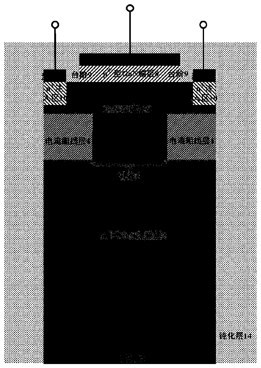
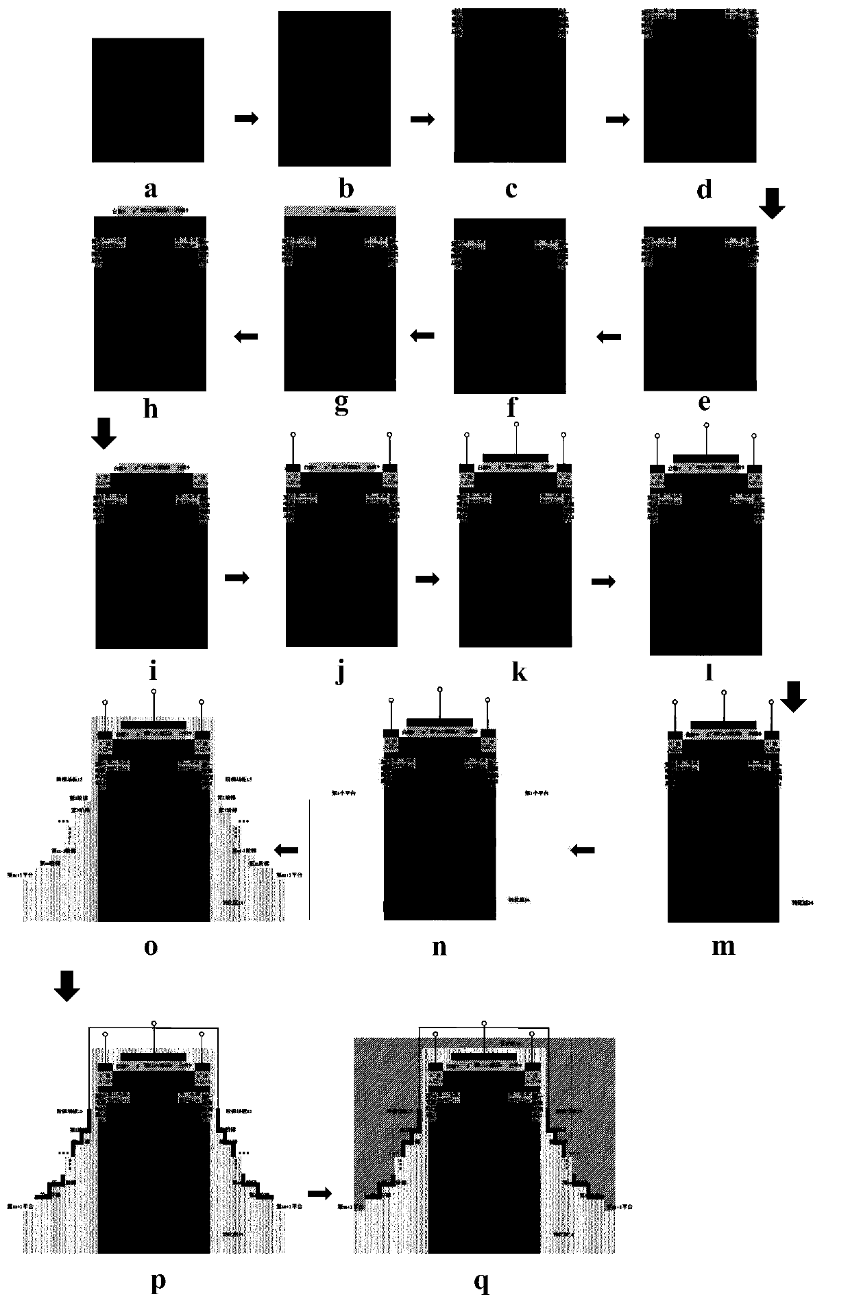
[0062] Embodiment 1: Fabricate a current aperture heterojunction field effect device in which both the passivation layer and the protective layer are SiN, and the step number of the step field plate is 1.

[0063] Step 1. Epitaxial n on the substrate - type GaN, forming n - type GaN drift layer 2, such as image 3 a.

[0064] Using metal-organic chemical vapor deposition techniques, the n + Type GaN substrate 1 with an epitaxial thickness of 100 μm and a doping concentration of 1×10 15 cm -3 the n - type GaN drift layer 2 .

[0065] The process conditions used for epitaxy are: the temperature is 950°C, the pressure is 40Torr, and the SiH 4 As the doping source, the flow rate of hydrogen gas is 4000 sccm, the flow rate of ammonia gas is 4000 sccm, and the flow rate of gallium source is 100 μmol / min.

[0066] Step 2. Epitaxial n-type GaN on the drift layer to form an n-type GaN aperture layer 3, such as image 3 b.

[0067] Using metal-organic chemical vapor deposition...

Embodiment 2

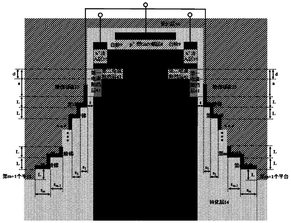
[0118] Embodiment 2: Both the passivation layer and the protective layer are made of SiO 2 , and the current aperture heterojunction field effect device with the step number of the step field plate being 2.

[0119] Step 1. Epitaxial n on the substrate - type GaN, forming n - type GaN drift layer 2, such as image 3 a.

[0120] At a temperature of 1000°C and a pressure of 45Torr, SiH 4 As the dopant source, the flow rate of hydrogen gas is 4400sccm, the flow rate of ammonia gas is 4400sccm, and the flow rate of gallium source is 110μmol / min, using metal organic chemical vapor deposition technology, at n + The epitaxial thickness on the GaN substrate 1 is 20 μm, and the doping concentration is 1×10 16 cm -3 the n - type GaN material, complete n - Type GaN drift layer 2 fabrication.

[0121] The second step. Epitaxial n-type GaN on the drift layer to form an n-type GaN aperture layer 3, such as image 3 b.

[0122] At a temperature of 1000°C and a pressure of 45Torr, ...

Embodiment 3

[0164] Embodiment three: making passivation layer is SiO 2 , the protective layer is SiN, and the number of steps of the step field plate is 4 current aperture heterojunction field effect devices.

[0165] Step A. The temperature is 950°C, the pressure is 40Torr, and SiH 4As the doping source, the flow rate of hydrogen gas is 4000 sccm, the flow rate of ammonia gas is 4000 sccm, and the process conditions of gallium source flow rate are 100 μmol / min, using metal organic chemical vapor deposition technology, at n + Type GaN substrate 1 with an epitaxial thickness of 3 μm and a doping concentration of 1×10 18 cm -3 the n - type GaN drift layer 2, such as image 3 a.

[0166] Step B. The temperature is 950°C, the pressure is 40Torr, and SiH 4 As the doping source, the flow rate of hydrogen gas is 4000 sccm, the flow rate of ammonia gas is 4000 sccm, and the process conditions of gallium source flow rate are 100 μmol / min, using metal organic chemical vapor deposition technol...


PUM


Abstract

The invention discloses an enhanced grid field plate GaN-based current aperture heterojunction field-effect device and a fabrication method thereof. The enhanced grid field plate GaN-based current aperture heterojunction field-effect device comprises an n<+> type GaN substrate (1), an n<-> type GaN drift layer (2), an n type GaN aperture layer (3), current blocking layers (4), a GaN channel layer (6) and a barrier layer (7), wherein sources (11) are deposited at two sides of the barrier layer, a p<+> type GaN cap layer (8) is arranged on the barrier layer between the sources, steps (9) are etched at two sides of the p<+> type GaN cap layer, a grid (12) is deposited on the p<+> type GaN cap layer, a drain (13) is deposited under the n<+> type GaN substrate, a passivation layer (14) wraps other regions except a bottom part of the drain, stepped field plates (15) are arranged at two sides of the passivation layer and are electrically connected with the grid, and a protection layer (16) is arranged on the passivation layer and the stepped field plates. The enhanced grid field plate GaN-based current aperture heterojunction field-effect device has the advantages of high breakdown voltage, simple process and small conduction resistance, and can be used for a power electronic system.

Description

technical field [0001] The invention belongs to the technical field of microelectronics, and relates to a semiconductor device, in particular to an enhanced grid field plate GaN-based current aperture heterojunction field effect device, which can be used in a power electronic system. [0002] technical background [0003] Power semiconductor devices are the core components of power electronics technology. As energy and environmental issues become increasingly prominent, research and development of new high-performance, low-loss power devices has become one of the effective ways to improve power utilization, save energy, and alleviate energy crises. In the research of power devices, there is a serious restrictive relationship between high speed, high voltage and low on-resistance. Reasonable and effective improvement of this restrictive relationship is the key to improving the overall performance of the device. With the development of microelectronics technology, the performan...

Claims


Application Information

Patent Timeline
Patent Type & Authority Patents(China)
IPC IPC(8): H01L29/06H01L29/40H01L21/335H01L29/778
CPCH01L29/0615H01L29/404H01L29/66462H01L29/7783H01L29/7786
Inventor 毛维石朋毫杜鸣郝跃王冲
Owner XIDIAN UNIV
Why Eureka
Try Eureka