Voltage buffer circuit and low dropout regulator (LDO) integrated with voltage buffer circuit
A voltage buffer and circuit technology, applied in instruments, regulating electrical variables, control/regulating systems, etc., can solve problems such as complex circuit structures, and achieve the effects of improving transient response, reducing costs, and reducing up-shooting peaks
- Summary
- Abstract
- Description
- Claims
- Application Information
AI Technical Summary
Problems solved by technology
Method used
Image
Examples
Embodiment Construction
[0026] The present invention will be further theoretically analyzed below in conjunction with the accompanying drawings and specific embodiments.
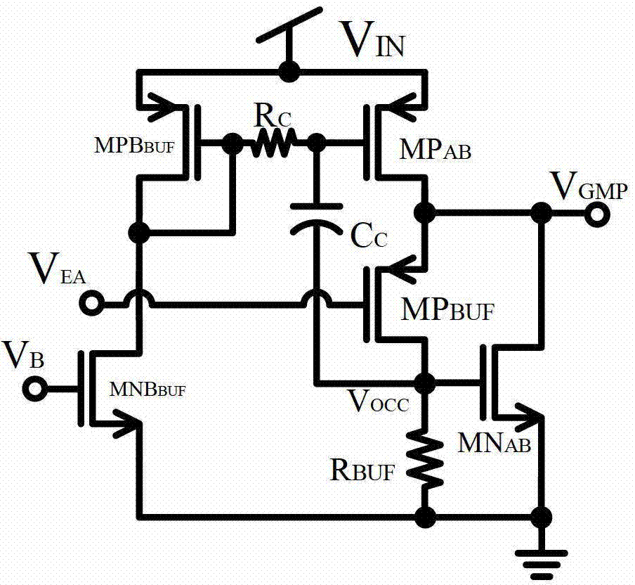
[0027] The voltage buffer circuit proposed by the present invention is essentially a push-pull output super source follower circuit (Super Class AB Source Follower Circuit, SSFC), figure 2 An implementation form is given, including: three PMOS transistors MP BUF , MPB BUF , MP AB , two NMOS tubes MN AB , MNB BUF , two resistors R C , R BUF , and a capacitor C C . MP BUF The gate of the EA op amp is connected to the output signal V EA , drain and resistor R BUF Connected at one end, R BUF Connect the other end to ground potential, MP BUF The source of the buffer output is connected to the gate V of the pass transistor GMP . MN AB The gate and MP BUF The drain is connected, and the drain is connected to the MP BUF The source is connected, MN AB The source is connected to ground potential, MN AB with MP BUF Consti...
PUM
 Abstract
Description
Claims
Application Information


