Manufacture method of depletion mode metal-oxide-semiconductor field effect transistor (MOSFET)
A manufacturing method and depletion-type technology, applied in semiconductor/solid-state device manufacturing, electrical components, circuits, etc., can solve problems such as inability to manufacture high-quality depletion-type MOSFETs and inaccurate channel depth control
- Summary
- Abstract
- Description
- Claims
- Application Information
AI Technical Summary
Problems solved by technology
Method used
Image
Examples
Embodiment Construction
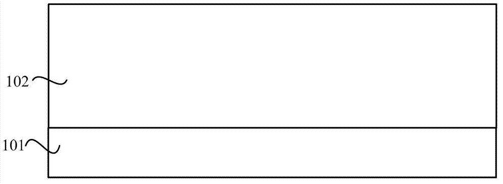
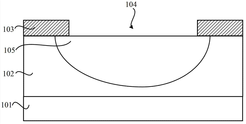
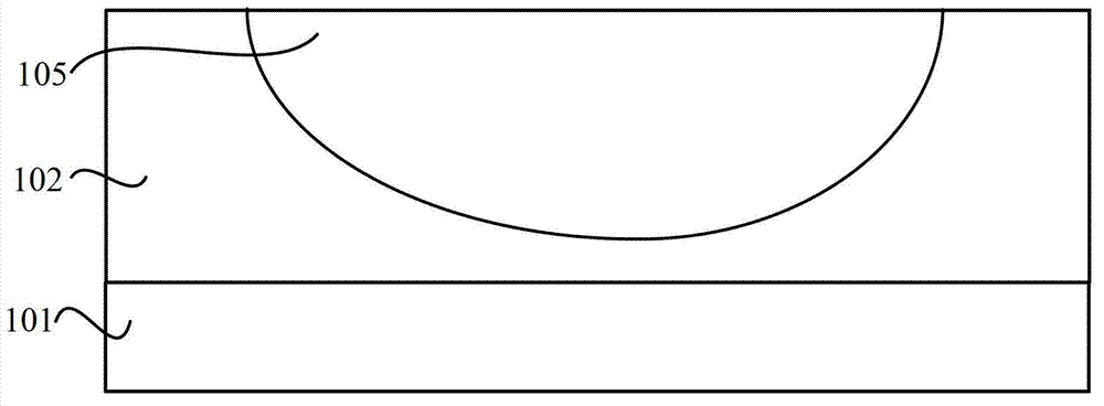
[0026] The core idea of the present invention is to use the mask layer to perform ion implantation to realize the channel of the depletion MOSFET. By using the mask layer, the position and structure of the channel can be precisely controlled, and the channel can be precisely controlled by adjusting the conditions of ion implantation. parameters such as depth and doping concentration. Precise trench structure, location, and depth enable high-performance depletion-mode MOSFETs.
[0027] In order to make the purpose, technical solution and advantages of the present invention more clear, the following will be further described in detail in conjunction with the accompanying drawings.
[0028] Such as Figure 7 As shown, the depletion MOSFET in one embodiment of the present invention includes: an N-type substrate 101; an N-type epitaxial layer 102 formed on one side of the substrate 101; a P-type epitaxial layer 102 formed in the N-type epitaxial layer 102 Doped deep well 105; N...
PUM
 Abstract
Description
Claims
Application Information


