Back contact layer structure, preparation method thereof and CdTe thin-film solar cell comprising back contact layer structure
A solar cell, back contact technology, applied in coatings, circuits, photovoltaic power generation, etc., to achieve effective cost control, improve intensification, and avoid environmental pollution
- Summary
- Abstract
- Description
- Claims
- Application Information
AI Technical Summary
Problems solved by technology
Method used
Image

Examples
Embodiment 1
[0045] A single growth chamber magnetron sputtering system is used to manufacture the back contact layer structure of the present invention. The advantages of using a single growth chamber magnetron sputtering system are simple equipment and diversified equipment functions. With the help of the single growth chamber magnetron sputtering system, the manufacturing process of the back contact layer structure is as follows:
[0046] First, perform the pretreatment of the surface of the CdTe film: open the gate of the growth chamber of the magnetron sputtering system, and the CdCl 2 The heat-treated CdTe film (supported on a glass substrate) sample is placed in the growth chamber of the magnetron sputtering system through a transfer rod, and the sample baffle is opened. The magnetron sputtering system has forward and reverse sputtering functions. A negative potential (1-3kV) is applied to the system substrate disk. The reverse sputtering function of the magnetron sputtering system is ...
Embodiment 2
[0051] A dual growth chamber magnetron sputtering system is used to manufacture the back contact layer structure of the present invention.
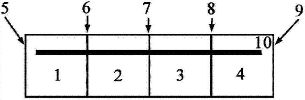
[0052] figure 2 It shows the structure diagram of the dual growth chamber DC magnetron sputtering system used for manufacturing the back contact layer structure according to the present invention. The dual DC magnetron sputtering growth chamber system includes: a magnetron sputtering first growth chamber 1, a first transition chamber 2, a magnetron sputtering second growth chamber 3, a second transition chamber 4, and a first growth chamber for sampling The gate 5, the first growth chamber sampling gate 6, the second growth chamber sampling gate 7, the second growth chamber sampling gate 8, the second transition chamber sampling gate 9 and the transfer rod 10. The advantage of using such a dual-growth-chamber DC magnetron sputtering system is that it can perform assembly line operation and improve production efficiency, and compared with Ex...
Embodiment 3
[0058] A dual growth chamber magnetron sputtering system is used to manufacture the back contact layer of the present invention. Compared with Example 2, the difference is that MoO 3 Target used as sputtering source to make MoO 3 Film (MoO 3 Buffer layer), therefore, only the formation of MoO is described below 3 The process of buffer layer, and omit the description of other same steps.
[0059] After the surface pretreatment of the CdTe thin film sample is optionally completed, the negative potential applied to the system substrate disk is removed, and the negative potential is applied to the MoO used for magnetron sputtering. 3 (5N purity) MoO is formed on the target by radio frequency sputtering 3 film. The atmosphere of magnetron sputtering is pure argon. The flow and pressure of argon are controlled and adjusted by the mass flowmeter of the magnetron sputtering system. The pressure is controlled at 0.45Pa, for an area of 100cm 2 For samples, the bombardment power is usually...
PUM
| Property | Measurement | Unit |
|---|---|---|
| thickness | aaaaa | aaaaa |
| thickness | aaaaa | aaaaa |
| thickness | aaaaa | aaaaa |
Abstract
Description
Claims
Application Information
 - R&D
- Intellectual Property
- Life Sciences
- Materials
- Tech Scout
- Unparalleled Data Quality
- Higher Quality Content
- 60% Fewer Hallucinations
Browse by: Latest US Patents, China's latest patents, Technical Efficacy Thesaurus, Application Domain, Technology Topic, Popular Technical Reports.
© 2025 PatSnap. All rights reserved.Legal|Privacy policy|Modern Slavery Act Transparency Statement|Sitemap|About US| Contact US: help@patsnap.com