Aluminum substrate used for packaging LED (Light Emitting Diode)

A technology of LED packaging and aluminum substrates, applied in electrical components, circuits, semiconductor devices, etc., can solve the problems of complex processing, low luminous efficiency, poor consistency, etc., and achieve the effects of good heat dissipation, improved luminous efficiency, and simplified processes

Inactive Publication Date: 2012-11-14
HANGZHOU DIANZI UNIV
View PDF4 Cites 17 Cited by
  • Summary
  • Abstract
  • Description
  • Claims
  • Application Information

AI Technical Summary

Problems solved by technology

[0004] The first technical problem to be solved by the present invention is to provide a preparation scheme for the insulating layer in the aluminum substrate used for LED packaging, improve the thermal conductivity of the insulating layer, and overcome the difficult heat dissipation, large light decay, and short life of SMD LEDs and other shortcomings
[0005] The second technical problem to be solved by the present invention is to provide an aluminum substrate for LED packaging, which solves the problems that the existing aluminum substrate needs mechanical slotting, grinding and polishing, resulting in complex processing, poor consistency, and low light efficiency.

Method used


Image

  • Aluminum substrate used for packaging LED (Light Emitting Diode)
  • Aluminum substrate used for packaging LED (Light Emitting Diode)
  • Aluminum substrate used for packaging LED (Light Emitting Diode)

Examples


Embodiment Construction

[0023] The principle and structure of the present invention will be further described below in conjunction with the accompanying drawings.

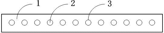
[0024] Such as figure 1 Shown is a top view of the aluminum substrate used for LED packaging in the embodiment of the present invention. According to the number of LED chips to be packaged, round holes are punched on the common aluminum plate 1 . The mirror aluminum plate 2 with the same length and width as the ordinary aluminum plate 1 is taken, and it is pressed at high temperature to become one body after pressing. The holes of the ordinary aluminum plate 1 and the mirror aluminum plate 2 form a circular groove 3 .

[0025] The ordinary aluminum plate 1 and the mirror aluminum plate 2 have the same shape and size.

[0026] The thermal conductivity of the mirror aluminum plate 2 is 1.3 times that of the ordinary aluminum plate 1, and has a good reflective effect, with a reflectivity of 85% and high tensile strength.

[0027] Such as ...


PUM

PropertyMeasurementUnit
particle sizeaaaaaaaaaa
thermal conductivityaaaaaaaaaa

Abstract

The invention relates to an aluminum substrate used for packaging an LED (Light Emitting Diode). The aluminum substrate comprises a common aluminium plate and a mirror plane plate which are laminated under high temperature. Through holes used for mounting LEDs are evenly arranged on the common aluminium plate which comprises, from top to bottom, a line layer, an insulated layer and a substrate. The insulated layer is made of epoxy resin, and alumina, carborundum, silicon dioxide and aluminum nitride which are nanoscale additives; the average particle size of the nanoscale additives is 40nm; and the purity of the nanoscale additives is above 99%. By adopting the aluminum substrate, a single chip or a plurality of chips can be packaged without being notched or polished and the substrate can be in any shape. The aluminum substrate has a flexible structure in application, is simple and practical, good in heat dissipation, simplified in process and high in light emitting efficiency.

Description

technical field [0001] The invention belongs to the technical field of LED packaging, in particular to an aluminum substrate used for LED packaging. Background technique [0002] Most of the LED packages of existing LED fluorescent lamps and street lamps use pre-packaged single LED light source devices, that is, chip LEDs, which are welded on the substrate for circuit connection and heat dissipation. Due to the existence of an insulating layer in this connection method, the main component of the insulating layer is generally resin, which leads to an increase in the number of heat transfer layers and an extension of the path between the LED chip and the substrate, thereby greatly reducing the speed at which the heat generated by the LED is emitted outward. , causing the operating temperature of the LED chip to rise. The rise in temperature will also bring about a series of problems such as accelerated aging of LED chips, increased light efficiency attenuation, reduced operat...

Claims


Application Information

Patent Timeline
Patent Type & Authority Applications(China)
IPC IPC(8): H01L33/48H01L33/60
Inventor 秦会斌祁姝琪
Owner HANGZHOU DIANZI UNIV
Why Eureka
Try Eureka